This review is written by non-expert and used for personal study only.
Real-time quantum error correction beyond break-even
- Quantum Information
Creating a reliable logical qubit requires a physical system with a vast state space and redundancy. This design ensures that logical information can be accurately transferred without distortion, even when physical errors occur. Bosonic codes, derived from a harmonic oscillator’s state space, have emerged as a promising alternative to the conventional approach using registers of physical qubits. However, control overhead has hindered current experiments from achieving a coherence time gain ($G$) for actively error-corrected logical qubits compared to the best passive qubit encoding in the same system.
Researchers have made progress with full code stabilization and error correction of logical qubits using $GKP$ encoding. This process involves converting a logical qubit into an oscillator’s grid states and implementing a ‘trickle-down’ quantum error correction (QEC) scheme based on prior research proposals. With low logical error probabilities and resulting lifetimes of logical Pauli eigenstates, this method has allowed the exploration of QEC processes on previously unattainable timescales.
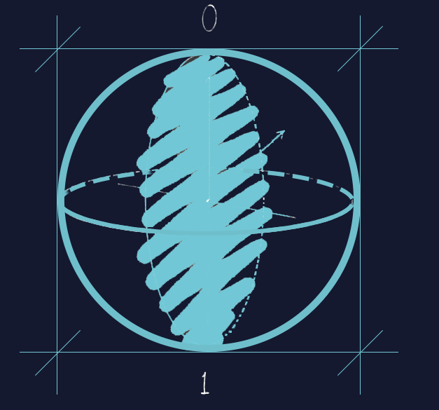
GKP
GKP encoding works by mapping a logical qubit onto an infinite-dimensional Hilbert space spanned by the eigenstates of a harmonic oscillator. This encoding allows for continuous-variable quantum error correction, which means that it can correct errors in the amplitude and phase of the encoded state.
One advantage of GKP encoding is that it can be implemented using simple linear optics and homodyne detection techniques, which are relatively easy to implement experimentally. Additionally, GKP encoding has been shown to have high fidelity and coherence gain compared to other types of quantum error-correcting codes.
To efficiently eliminate entropy from the system, an artificial error-correcting dissipation was used. This method focuses on prioritizing the correction of frequent small errors while still addressing rare large errors. The strategy reduces control overhead in grid code and has been demonstrated in other bosonic codes as well.
Grid code
A grid code is used to protect quantum information from decoherence. In a grid code, a logical qubit is encoded into an infinite-dimensional Hilbert space spanned by the eigenstates of a harmonic oscillator. The code states are defined as superpositions of coherent states, which are displaced versions of the oscillator ground state. These coherent states are arranged in a grid-like pattern in phase space, with each point on the grid representing a different encoded state.
Grid codes have several advantages over other types of quantum error-correcting codes. For example, they can be implemented using simple linear optics and homodyne detection techniques, which are relatively easy to implement experimentally. Additionally, they have been shown to have high fidelity and coherence gain compared to other types of quantum error-correcting codes.
Bosonic code
In a bosonic code, a logical qubit is encoded into a collection of bosonic modes. The code states are defined as superpositions of Fock states, which represent different numbers of photons in each mode. These Fock states are arranged in a specific pattern that allows for error correction and detection.
Bosonic codes have several advantages over other types of quantum error-correcting codes. For example, they can be implemented using simple linear optics and photon counting techniques, which are relatively easy to implement experimentally. Additionally, they have been shown to have high fidelity and coherence gain compared to other types of quantum error-correcting codes
Researchers have constructed a rank-4 error correction channel using a single auxiliary qubit and classical controller. This is accomplished by implementing two rank-2 dissipators that guide the system towards the +1 eigenspace of the finite-energy code stabilizers. The dissipation channel implementation consists of qubit rotations, oscillator displacements, conditional rotations, and virtual oscillator rotations.
Rank
The rank of an error correction channel refers to the number of independent errors that can be corrected by the channel. In general, an error correction channel is a quantum operation that maps a noisy quantum state to a corrected quantum state. The goal of quantum error correction is to design channels that can correct errors caused by decoherence and other sources of noise.
The rank of an error correction channel is an important parameter because it determines how many errors can be corrected by the channel. A higher rank means that more independent errors can be corrected, which leads to better performance in practice.
To enhance the performance of QEC, a real-time reinforcement learning (RL) agent is employed. The RL agent is trained using a logical Pauli eigenstate and a candidate QEC protocol, allowing it to find a QEC protocol that results in the longest logical qubit lifetime. The RL agent can learn the optimal value of the large intermediate displacement without a model, enhancing QEC performance at the expense of a considerably slower gate.
The best-performing QEC circuit is then selected for further analysis, emphasizing its capacity to create high-quality quantum memory. The average channel fidelity serves as a metric to quantify the deviation of any quantum channel from the identity.
Both types of qubits exhibit different fidelity decay rates due to amplitude damping and white-noise dephasing channels, with one type experiencing a higher fidelity decay constant. Grid states encoding for qubits incurs an immediate penalty in fidelity decay rate, eventually leading grid states away from the logical manifold and towards the vacuum state.
Error-correcting dissipation stabilizes the grid-code manifold, resulting in a logical Pauli channel with lifetimes of logical Pauli eigenstates. This leads to a coherence gain, confidently surpassing the break-even point.
The QEC process is investigated by measuring auxiliary qubit outcomes, known as syndromes, which offer insights into the stochastic path taken during each cycle. A simplified model of trickle-down dissipation is used to interpret the dataset, with the $g$ outcome indicating projection onto the code space and the $e$ outcome signifying partial or complete error correction. This dataset provides valuable information about the QEC process that was previously unattainable.
Real-time error correction has been utilized to create a stable logical qubit with a longer lifetime than passive qubit encoding, rendering QEC a practical tool for enhancing quantum memories. Challenges in grid-code QEC include occasional collapses of logical performance due to spurious degrees of freedom in the system. Future developments should incorporate robustness against auxiliary qubit bit flips, either through path-independent control or by adopting an auxiliary qubit with biased noise.
After initial state correction, the QEC process settles into a dynamic equilibrium that persists for at least a hundred thousand cycles without any significant increase in error rates over time. Residual deviations from stationarity are caused by transmon leakage to states higher than $|f\rangle$ at a rate of $1.3 \times 10^{−4}$ per cycle.
Physical errors in the quantum state are prevented from accumulating and causing logical errors by low-rank error-correcting dissipation. The process successfully corrects $97%$ of errors. Rare large errors require several cycles to be corrected, resulting in a weakly time-correlated QEC process and lasting traces of outcomes generated by large-distance errors.
Post-selection of trajectories with different syndrome patterns can improve the fidelity lifetime of logical states in quantum computing. This method can eliminate both small and large errors, but with varying rejection probabilities per cycle.
Real-time error correction has been used to create a stable logical qubit with a longer lifetime than passive qubit encoding, making QEC a practical tool for enhancing quantum memories. Previous QEC experiments only protected certain Pauli operators and did not protect the logical identity operator $I_L$. Challenges in grid-code QEC include occasional collapses of logical performance due to spurious degrees of freedom in the system, which could be mitigated by adopting a tunable auxiliary qubit and periodically re-training the QEC circuit. As quantum computing advances, future development should focus on incorporating robustness against auxiliary qubit bit flips, either through path-independent control or by adopting an auxiliary qubit with biased noise. This will help to further improve the stability and reliability of logical qubits, paving the way for more advanced quantum technologies.
Required Additional Study Materials
- “Quantum Error Correction” by Daniel A. Lidar and Todd A
- Joschka Roffe (2019) Quantum error correction: an introductory guide, Contemporary Physics, 60:3, 226-245, DOI: 10.1080/00107514.2019.1667078
Reference
Sivak, V.V., Eickbusch, A., Royer, B. et al. Real-time quantum error correction beyond break-even. Nature 616, 50–55 (2023).
Beating the break-even point with a discrete-variable-encoded logical qubit
- Quantum Information
Decoherence, which is the loss of quantum coherence, is a significant challenge in building quantum computers. However, quantum error correction (QEC) methods can help overcome this issue. Although QEC schemes have been shown to work in various systems, we need to increase the lifetime of logical qubits (the basic units of quantum information) to improve quantum information storage and processing. One promising approach for fault-tolerant quantum computation is using discrete-variable qubits encoded with mutually orthogonal Fock states (particular quantum states of an oscillator). However, increasing the lifetime of these encoded logical qubits remains a challenge.
Fock states
In quantum mechanics, a Fock state is a type of quantum state that describes the number of particles in a given mode of a quantum field. Specifically, a Fock state $|n\rangle$ represents a state with exactly $n$ particles in the mode.
Fock states are important in many areas of quantum physics, including quantum optics and quantum information processing. In particular, they are used to describe the states of photons in optical systems and the states of phonons in mechanical systems.
In optical systems, Fock states are often used to describe the number of photons in a given mode of an electromagnetic field. For example, a single-photon Fock state $|1\rangle$ represents a state with exactly one photon in the mode. These states can be used to encode information for applications such as quantum communication and cryptography.
In mechanical systems, Fock states can be used to describe the vibrational modes of mechanical resonators such as nanomechanical oscillators or superconducting resonators. These systems can be used for applications such as sensing and signal processing.
Real-time feedback correction, which is a method that adjusts the system based on the error information, goes beyond the minimum requirements for a successful QEC in a photonic qubit placed in a microwave cavity (a container that can hold electromagnetic waves). This ensures that code words (sequences of qubits that encode information) stay distinguishable from each other. The error-detection process used in this approach allows QEC codes to handle the loss of more than one photon. This process includes encoding quantum information, measuring error syndrome (identifying what errors have occurred), correcting errors in real-time, and decoding the information.
The experiments in this study use a combination of a superconducting transmon qubit and a microwave cavity to control multiple photon states for QEC effectively. The error syndrome measurement is done through a projection measurement scheme, which uses a classical microwave pulse. This method has potential benefits for adapting to different error types and being sensitive to small errors in the qubits.
The QEC process can be implemented for the binomial code (a specific encoding scheme), but some practical imperfections limit its performance. The QEC method with binomially encoded logical qubits can protect against single-photon-jump errors (errors caused by the loss of one photon) through continuous error detection and correction.
Binomial code
Binomial code is used to protect quantum information stored in bosonic systems, such as microwave cavities or optical fibers. In the binomial code, the logical qubit is encoded in photon-number states of a cavity, and the error syndrome is determined by the parity of the photon number.
Specifically, when a single-photon-loss error occurs, the quantum information is projected into an error space spanned by two states: $|0\rangle$ and $|1\rangle$. These states correspond to even and odd photon numbers, respectively. The parity of the photon number acts as the error syndrome to distinguish these two spaces.
The binomial code is a stabilizer code, which means that it can detect and correct errors without measuring the state of the logical qubit directly. Instead, measurements are made on ancillary qubits that are entangled with the logical qubit. These measurements allow for real-time correction operations to be applied to recover quantum information stored in the cavity.
These imperfections include a probability of losing two photons during idle time, interference between single-photon-loss errors and self-Kerr interaction (a nonlinear optical effect), and imperfect recovery operations at the quantum level. To mitigate these imperfections, some strategies include choosing an optimal waiting time, using a two-layer QEC process (a more advanced error correction method), and adopting the photon-number-resolved a.c. Stark shift (PASS) method during idle operations.
Self-Kerr interaction
The Self-Kerr interaction is a type of nonlinear optical effect that occurs when light interacts with a material medium. In this interaction, the intensity of the light changes the refractive index of the medium, which in turn affects the propagation of the light. Specifically, as the intensity of the light increases, so does the refractive index of the medium. This causes a self-focusing effect, where light waves are focused to a smaller spot size than they would be in a linear medium.
Stark shift method
It is the method to mitigate the effects of photon loss-induced dephasing in logical qubits. This technique is named after the Stark effect, which is a phenomenon in atomic physics where an external electric field causes a shift in the energy levels of an atom.
In the PASS method, an off-resonant drive pulse with a frequency detuning is applied to an auxiliary qubit during the idle operation. This results in different phase accumulation rates for Fock states with different photon numbers relative to the vacuum state. By choosing an optimal amplitude of the detuned drive, it is possible to achieve an error-transparent condition that mitigates the dephasing effect of the logical qubit.
The effectiveness of a QEC procedure is measured by the process fidelity, which compares the actual outcome with the ideal outcome. Without a QEC operation, the inability to protect quantum information from single-photon-loss errors reduces the process fidelity to 0.73. However, using one-layer and two-layer QECs can improve this value. The measured process fidelities for the corrected binomial code with one-layer and two-layer QECs show a slow decay, indicating an improvement over the minimum requirements for a successful QEC by factors of 1.2 and 2.9, respectively.
This study demonstrates a way to increase the coherence time of quantum information encoded with discrete variables by using repetitive QEC. The main source of inaccuracy comes from the two-photon-loss error, which can be corrected by higher-order binomial codes. This research provides practical guidance for optimizing quantum control systems and designing QEC procedures for future applications of logical qubits, making it more accessible for physics undergraduate students.
Required Additional Study Materials
- “Quantum Error Correction” by Daniel A. Lidar and Todd A
- Joschka Roffe (2019) Quantum error correction: an introductory guide, Contemporary Physics, 60:3, 226-245, DOI: 10.1080/00107514.2019.1667078
Reference
Ni, Z., Li, S., Deng, X. et al. Beating the break-even point with a discrete-variable-encoded logical qubit. Nature 616, 56–60 (2023).
Gate-tunable heavy fermions in a moire Kondo lattice
- Quantum Simulation
Moiré superlattices, which are formed by overlapping two periodic lattices, have sparked interest due to their flat electronic bands that lead to correlated insulating, magnetic, and superconducting states. One particularly intriguing possibility is the creation of a moiré Kondo lattice, a complex electron system that could provide valuable insights into the behavior of electrons in these materials.
In an experiment, researchers demonstrated a moiré Kondo lattice using AB-stacked $\text{MoTe}_2\text{/WSe}_2$ bilayers. These bilayers were doped with holes, or empty spaces for electrons, to create a triangular moiré pattern with a period of about $5 nm$. Holes in the $\text{MoTe}_2$ layer can be localized, meaning they remain stationary, while holes in the $\text{WSe}_2$ layer are mobile, free to move throughout the material.
Dual-gated devices enable scientists to independently fine-tune the electrostatic doping density and electric field in bilayers, resulting in topological phase transitions at specific doping values (v=1 and v=2) when the electronic bands invert. The Kondo lattice becomes observable before the band inversion occurs within particular regions of the doping and electric field phase diagram.
By separating local moments (localized electron spins) and conduction holes (mobile charge carriers) into distinct layers, researchers can achieve remarkable control over the system’s properties. This separation enhances the Kondo coupling effect, an interaction between localized spins and mobile charge carriers, leading to a large Fermi surface with heavy quasi-particle masses. The onset temperature for Kondo screening, the point at which the Kondo effect becomes noticeable, increases with the strengthening of the Kondo coupling effect and conduction hole density. To identify the Kondo lattice region, scientists employed magneto-transport and optical spectroscopy measurements. They measured the resistance of the material as a function of doping and electric field under specific experimental conditions, such as an out-of-plane magnetic field and low temperature. By analyzing the data, they were able to estimate the size of various energy gaps, the quasi-particle mass, and other properties in different regions of the phase diagram.
The coexistence of a significant energy gap in $\text{MoTe}_2$ and mobile holes in \text{WSe}_2 provides the necessary components for a Kondo lattice. This combination could lead to the emergence of a heavy-fermion liquid, an exotic state of matter characterized by strongly interacting electrons.
The temperature dependence of resistance in different regions revealed interesting behavior, including the emergence of heavy fermions in one region. By measuring the Hall resistance, researchers could determine the size of the Fermi surface and the behavior of the charge carriers in the system under various conditions.
Furthermore, the experiment demonstrated that the Kondo effect could be continuously tuned by doping and electric field. A more pronounced enhancement was observed when the $\text{WSe}_2$ band was close to the $\text{MoTe}_2$ lower Hubbard band. The observed asymmetry in the two Hubbard bands suggests that additional interaction mechanisms may be necessary to accurately describe the system.
Scientists have observed a gate-tunable Kondo effect and heavy-fermion liquid with a large Fermi surface in $\text{MoTe}_2\text{/WSe}_2$ moiré bilayers under specific conditions. This discovery offers exciting opportunities for further research into the gate-controlled Kondo destruction transition, which could have important implications for our understanding of complex electronic systems and potential applications in next-generation electronic devices.
Required Additional Study Materials
- “Many-Body Physics: From Kondo to Hubbard” by Eva Pavarini, Erik Koch and Piers Coleman
- “The Kondo Lattice Model” by M. Lavagna and C. P´epin, https://doi.org/10.48550/arXiv.cond-mat/9903093
Reference
Zhao, W., Shen, B., Tao, Z. et al. Gate-tunable heavy fermions in a moiré Kondo lattice. Nature 616, 61–65 (2023).
2D fin field-effect transistors integrated with epitaxial high-k gate oxide
- Two-dimensional Materials
Advancements in integrated circuit technology depend on making transistors smaller, but traditional silicon-based structures face challenges when they reach sizes below 5 nanometers. High-mobility 2D layered semiconductors show potential to serve as the building blocks of next-generation ultra-small transistors, allowing for powerful electronic devices with intricate vertical designs.
Researchers have developed a method to create extremely thin layers of a material called $\text{Bi}_2\text{O}_2\text{Se}$ integrated with another material, $\text{Bi}_2\text{SeO}_5$, on insulating substrates. These structures have atomically flat interfaces, allowing for the fabrication of efficient transistors known as FinFETs. $\text{Bi}_2\text{O}_2\text{Se}$ was chosen for its unique structure, high electron mobility, moderate bandgap, excellent stability, and compatibility with Bi2SeO5.
These extremely thin $\text{Bi}_2\text{O}_2\text{Se}$ fins display remarkable mechanical strength and a high aspect ratio, which can be attributed to their anisotropic growth and the presence of dangling bonds on their surfaces. By adjusting the substrate’s symmetry, researchers can control the growth of these thin fins on insulating oxide substrates. They’ve successfully grown fins on various surfaces, such as $\text{CaF}_2$, $\text{LaAlO}_3$, $\text{SrTiO}_3$, and $\text{KTaO}_3$.
These structures maintain their shape after a native-oxide dielectric layer is integrated through a process involving UV-assisted intercalative oxidation. This native-oxide layer, $\text{Bi}_2\text{SeO}_5$, has a high dielectric constant (relative permittivity of approximately 21), making it ideal for electronic applications. Detailed microscopic investigations reveal the layered structure of $\text{Bi}_2\text{O}_2\text{Se}$ and $\text{Bi}_2\text{SeO}_5$, as well as their atomically flat interfaces.
Intercalative oxidation
Intercalative oxidation is a chemical process in which an oxidizing agent penetrates between the layers of a layered material, causing a change in its chemical composition and structure. This process is particularly important in the context of two-dimensional (2D) layered materials, as it allows researchers to precisely control and modify the properties of these materials for various applications, such as in transistors and other electronic devices.
In the case of 2D layered semiconductors, intercalative oxidation can be used to create ultrathin layers with specific properties. During this process, an oxidizing agent, such as oxygen or ozone, is introduced between the layers of the material. The oxidizing agent reacts with the material, altering its chemical composition and, in turn, its electronic properties.
One key advantage of intercalative oxidation is that it allows for the controlled and precise modification of layered materials. By carefully controlling the conditions under which the oxidation process takes place (e.g., temperature, pressure, and concentration of the oxidizing agent), researchers can achieve a desired level of oxidation and the corresponding changes in material properties.
High-resolution STEM images show extremely sharp interfaces in these structures on $\text{LaAlO}_3$ (100) substrate surfaces. By carefully controlling the oxidation process, researchers can create ultrathin 2D fins that enable the construction of advanced transistor devices such as FinFETs, VGAA transistors, and VTFETs. Lattice strain at the top interface of these structures does not impair performance due to the high-quality interfaces of the vertical sidewalls.
For the future of integrated circuits, it is crucial to develop robust, wafer-scale 2D fin arrays and integrate them with high-k oxide dielectrics. Researchers achieved this by forming 2D $\text{Bi}_2\text{O}_2\text{Se/Bi}_2\text{SeO}_5$ fin-oxide arrays on a 1-inch $MgO$ (110) wafer, featuring vertically aligned structures. Site-specific and high-density growth of these arrays is essential for large-scale fabrication and compact integration. This approach allows for small spacing between the fins, meeting the requirements of advanced technology nodes.
These 2D fin-oxide structures enhance the performance and reliability of FinFET devices. Researchers fabricated vertical 2D $\text{Bi}_2\text{O}_2\text{Se/Bi}_2\text{SeO}_5\text{/HfO}_2$ FinFETs with varying channel lengths, demonstrating excellent electrostatic control. The epitaxial high-k native-oxide $\text{Bi}_2\text{SeO}_5$ ensures high device reproducibility and improves various electronic properties. These FinFETs achieved a higher on-state current compared to other reported devices using 2D materials.
The wafer-scale 2D $\text{Bi}_2\text{O}_2\text{Se}$ fin arrays integrated with high-k \text{Bi}_2\text{SeO}_5$ dielectric meet the requirements for advanced transistors and could potentially extend Moore’s law with further optimization. This innovative approach to 2D fin-oxide structures promises to advance the development of integrated circuits and enable the next generation of high-performance and ultra-scaled transistors.
Required Additional Study Materials
- Wang, S., Liu, X. & Zhou, P. The road for 2D semiconductors in the silicon age. Adv. Mater. 34, 2106886 (2022).
- Shen, Y. et al. The trend of 2D transistors toward integrated circuits: scaling down and new mechanisms. Adv. Mater. 34, 2201916 (2022).
- Liu, C. et al. Two-dimensional materials for next-generation computing technologies. Nat. Nanotechnol. 15, 545–557 (2020).
- Akinwande, D. et al. Graphene and two-dimensional materials for silicon technology. Nature 573, 507–518 (2019).
- Chhowalla, M., Jena, D. & Zhang, H. Two-dimensional semiconductors for transistors. Nat. Rev. Mater. 1, 16052 (2016).
- Illarionov, Y. Y. et al. Insulators for 2D nanoelectronics: the gap to bridge. Nat. Commun. 11, 3385 (2020).
- Das, S. et al. Transistors based on two-dimensional materials for future integrated circuits. Nat. Electron. 4, 786–799 (2021).
Reference
Tan, C., Yu, M., Tang, J. et al. 2D fin field-effect transistors integrated with epitaxial high-k gate oxide. Nature 616, 66–72 (2023).
Deforming lanthanum trihydride for superionic conduction
- Electrochemistry
Solid materials that conduct a variety of ions have important applications in devices like batteries, fuel cells, and sensors. Some of these materials can transition into what is called a superionic state, which is characterized by high conductivity and low barriers for ion movement. This makes them ideal for use as solid electrolytes. Researchers have been studying hydride ion conductors, a type of material that conducts negatively charged hydrogen ions ($\text{H-}$), for new battery and fuel cell technologies. However, none of these materials have shown superionic conduction at room temperature.
This research focuses on a specific type of material called rare earth element trihydrides ($\text{REHx}$). These materials are interesting because they exhibit rapid movement of H- ions and strong conduction of electrons. To create samples of a rare earth hydride called $LaHx$, scientists used a technique called high-energy ball milling. This method produces numerous tiny grains and lattice defects, which can be used to change the material’s electronic conductivity. The researchers used various imaging techniques to study the samples and found that they had many grain boundaries (regions where grains meet) and tiny areas with different crystal structures or no crystal structure at all.
Lattice disorder, which refers to irregularities in the arrangement of atoms in a material, can negatively affect electron conduction in metals and semiconductors. This is because electrons can scatter at surfaces, grain boundaries, or areas where the crystal structure doesn’t match up properly. The $\text{LaHx}$ samples created in this study have many grain boundaries and lattice disorder, which actually helps to scatter electrons and lower the material’s electronic conductivity. By deforming the lattice of $REHx$ materials, the researchers were able to create samples with low electronic conductivity but still allowed H- ions to move easily.
Grain boundaries Grain boundaries are the interfaces or regions that separate individual crystalline grains (also known as crystallites) within a polycrystalline material. In other words, grain boundaries are the areas where two or more crystals meet within a solid. Each grain has a specific orientation and crystal structure, and grain boundaries occur when these grains with different orientations come into contact with one another.
Grain boundaries can have significant effects on the mechanical, electrical, and thermal properties of materials. This is because the atoms at the grain boundaries have different arrangements and bonding compared to those in the bulk of the grains. As a result, grain boundaries can act as barriers to the movement of atoms, electrons, and other particles within the material.
Some of the effects of grain boundaries on material properties include:
- Mechanical properties: Grain boundaries can influence a material’s strength and ductility. Generally, smaller grain sizes lead to stronger materials because there are more grain boundaries that can impede the movement of dislocations, which are line defects in the crystal structure. This phenomenon is known as grain boundary strengthening or the Hall-Petch effect.
- Electrical properties: Grain boundaries can impact the electrical conductivity of materials. In metals, grain boundaries can scatter electrons, which may increase the electrical resistivity. In semiconductors, grain boundaries may trap charge carriers, which can lead to decreased electrical conductivity and increased recombination of electrons and holes.
- Thermal properties: The thermal conductivity of materials can also be affected by grain boundaries. Similar to the electrical properties, grain boundaries can scatter phonons, the primary heat carriers in materials, leading to reduced thermal conductivity.
- Diffusion: Grain boundaries can act as pathways for the diffusion of atoms or particles in a material. Diffusion can be faster along grain boundaries compared to the bulk of the grains because the atomic arrangement at the boundaries is less ordered, creating more available space for atoms to move.
The ability of $LaHx$ to conduct H- ions depends on the extent to which its lattice is deformed. This property provides an opportunity to control both electron and H- ion conduction in these materials. The superionic behavior of $LaHx$, which is its ability to conduct ions very efficiently, is due to the small differences in energy needed for H- ions to move between different positions in the lattice and the short distances between these positions.
This research has shown that deforming the lattice of $LaHx$ can enable the development of metal hydride batteries that work at room temperature or even lower. Several H- conductors have been created with high ionic conductivity over a wide temperature range. This opens up possibilities for investigating and using H- conductors in various applications related to energy storage and chemical conversion.
Deforming the lattice of $REHx$ materials reduces electron conduction while allowing H- ions to move easily. This leads to a significant decrease in electronic conductivity, making these materials promising candidates for use in devices like batteries and fuel cells. By extending this approach to other hydride materials, researchers could discover a wider range of materials suitable for conducting H- ions.
Required Additional Study Materials
- Bachman, J. C. et al. Inorganic solid-state electrolytes for lithium batteries: mechanisms and properties governing ion conduction. Chem. Rev. 116, 140–162 (2016).
- Zhang, Z. et al. New horizons for inorganic solid state ion conductors. Energy Environ. Sci. 11, 1945–1976 (2018).
- Munoz, R. C. & Arenas, C. Size effects and charge transport in metals: quantum theory of the resistivity of nanometric metallic structures arising from electron scattering by grain boundaries and by rough surfaces. Appl. Phys. Rev. 4, 011102 (2017).
Reference
Zhang, W., Cui, J., Wang, S. et al. Deforming lanthanum trihydride for superionic conduction. Nature 616, 73–76 (2023).
A LaCl3-based lithium superionic conductor compatible with lithium metal
- Batteries
All-solid-state lithium metal batteries (ASSLMBs) are a type of battery that requires solid electrolytes (SEs) with specific characteristics. These SEs need to have high ionic conductivity, a flexible lattice, and a broad electrochemical window to ensure compatibility with the battery’s electrodes. However, no single SE has been found to possess all these attributes, which has led to compatibility problems in earlier inorganic SEs. Researchers are actively seeking a lithium superionic conductor that possesses these essential properties for optimal ASSLMB performance.
Ionic conductivity
Ionic conductivity refers to the ability of a material to transport charged particles, or ions, through its structure. This property is crucial in electrochemical devices such as batteries, fuel cells, and supercapacitors, where ions need to move between electrodes through the electrolyte to facilitate charge transfer and enable the device to function.
In a material with high ionic conductivity, ions can move freely and quickly, resulting in efficient charge transfer and better performance of the electrochemical device. Conversely, low ionic conductivity can lead to slower charge transfer, reduced performance, and in some cases, device failure.
Li+ conduction in inorganic solid electrolytes (SEs) is influenced by the lattice structure. Researchers proposed a $\text{LaCl}_3$ lattice, a unique arrangement of atoms, featuring a non-close-packed anion lattice and one-dimensional (1D) channels for Li+ conduction. By connecting 1D channels through vacancies in the La atoms, a 3D Li-diffusion lattice can be created. Advanced computational simulations called ab initio molecular dynamics showed fast Li+ conduction in the $\text{LaCl}_3$ lattice at room temperature.
To further enhance the properties of the electrolyte, high-valence Ta5+ ions were introduced, creating vacancies in the lattice. The $Li_xTa_yLa_zCl_3$ composition was developed to maintain electrical neutrality within the doped lattice. The optimized $Li_{0.388}Ta_{0.238}La_{0.475}Cl_3$ SE demonstrated comparable room temperature ionic conductivity, but a lower activation energy (Ea), which is beneficial for ionic conductivity at low temperatures.
To investigate the Li+ chemical environments in the SEs, solid-state nuclear magnetic resonance (NMR) was employed. Two distinct peaks in the NMR spectra revealed the presence of Li1 ions in the channels and Li2 ions near La-vacancy sites. Analysis of Li+ content showed that Li+ ions preferentially occupy La-vacancy sites, and ultrafast Li+ exchange between these two types of sites was observed.
The structure of the $Li_{0.388}Ta_{0.238}La_{0.475}Cl_3$ electrolyte was determined using advanced X-ray and neutron diffraction techniques. Li+ ions were confirmed to occupy two types of sites in the lattice: Li1 in channels and Li2 near La sites. Using computational simulations, researchers found that the [Li1-Li2-Li1] chain was the most energetically favorable path for Li+ ions to move through the lattice. Doping with Ta5+ ions helped connect 1D channels in the $\text{LaCl}_3$ lattice, improving its overall performance.
An electrolyte pellet made of $Li_{0.388}Ta_{0.238}La_{0.475}Cl_3$ with many nanocrystalline defects was found to enhance interfacial stability against Li metal. This chloride electrolyte outperformed previous inorganic SE-based batteries in terms of cycling duration and areal capacity, showing better interfacial stability against Li metal. The $Li_{0.388}Ta_{0.238}La_{0.475}Cl_3$ electrolyte displayed uniform Li plating/stripping at the Li/SE interface due to a homogeneous distribution of Li+ ions.
The low electronic conductivity of $Li_{0.388}Ta_{0.238}La_{0.475}Cl_3$ prevented the growth of Li dendrites, ensuring a high critical current density. This electrolyte performed well in a full cell with a Li metal anode and an uncoated NCM523 cathode, cycling for over 100 cycles with 81.6% capacity retention. The LaCl3-based electrolyte enabled the development of ASSLMB without an additional buffer layer and achieved a charge voltage of up to 4.35 V, surpassing the stable electrochemical window of 4.27 V.
LaCl3-based electrolytes can accommodate a wide range of ions with various valences, from +1 to +6, at a high doping ratio of 33.34%. This offers immense potential for enhancing the electrolyte’s properties through the introduction of different doping ions. The design strategy can be extended to other lanthanide metal chlorides, and the resulting $Li_{0.388}Ta_{0.238}La_{0.475}Cl_3$ electrolytes still retain the desired lattice characteristics with rapid Li+ conduction.
Researchers have reported a LaCl3-based lithium superionic conductor with exceptional ionic conductivity and electrode compatibility. This development enabled stable cycling of a $Li/Li_{0.388}Ta_{0.238}La_{0.475}Cl_3/NCM523$ full cell with an areal capacity of $1.16$ mAh cm−2. The work also inspired a new family of UCl3-type SE systems based on $\text{LnCl}_3$ lattice (Ln = La, Ce, Nd, Sm, and Gd) with multiple element-doping options. This research represents a significant step forward in understanding and developing advanced electrolytes for all-solid-state lithium metal batteries, making them more accessible and efficient for a wide range of applications.
Required Additional Study Materials
- Famprikis, T., Canepa, P., Dawson, J. A., Islam, M. S. & Masquelier, C. Fundamentals of inorganic solid-state electrolytes for batteries. Nat. Mater. 18, 1278–1291 (2019).
- Manthiram, A., Yu, X. W. & Wang, S. F. Lithium battery chemistries enabled by solid-state electrolytes. Nat. Rev. Mater. 2, 16103 (2017).
- Tan, D. H. S., Banerjee, A., Chen, Z. & Meng, Y. S. From nanoscale interface characterization to sustainable energy storage using all-solid-state batteries. Nat. Nanotechnol. 15, 170–180 (2020).
- Bachman, J. C. et al. Inorganic solid-state electrolytes for lithium batteries: mechanisms and properties governing ion conduction. Chem. Rev. 116, 140–162 (2016).
- Lu, Y. et al. Critical current density in solid-state lithium metal batteries: mechanism, influences, and strategies. Adv. Funct. Mater. 31, 2009925 (2021).
- Chen, S. J. et al. Sulfide solid electrolytes for all-solid-state lithium batteries: structure, conductivity, stability and application. Energy Storage Mater. 14, 58–74 (2018).
- Wang, C. W. et al. Garnet-type solid-state electrolytes: materials, interfaces, and batteries. Chem. Rev. 120, 4257–4300 (2020).
- Wang, Y. et al. Doping strategy and mechanism for oxide and sulfide solid electrolytes with high ionic conductivity. J. Mater. Chem. A 10, 4517–4532 (2022).
Reference
Yin, YC., Yang, JT., Luo, JD. et al. A LaCl3-based lithium superionic conductor compatible with lithium metal. Nature 616, 77–83 (2023).
Leave a comment