This review is written by non-expert and used for personal study only.
Determining the gluonic gravitational form factors of the proton
- Experimental Particle Physics
The study focuses on understanding the gluonic gravitational form factors of the proton. To understand what this means, it’s helpful to first understand some background information about particle physics.
The proton is a subatomic particle that is composed of smaller particles called quarks and gluons. Quarks are held together by gluons, which are the carriers of the strong nuclear force that binds protons and neutrons together in atomic nuclei.

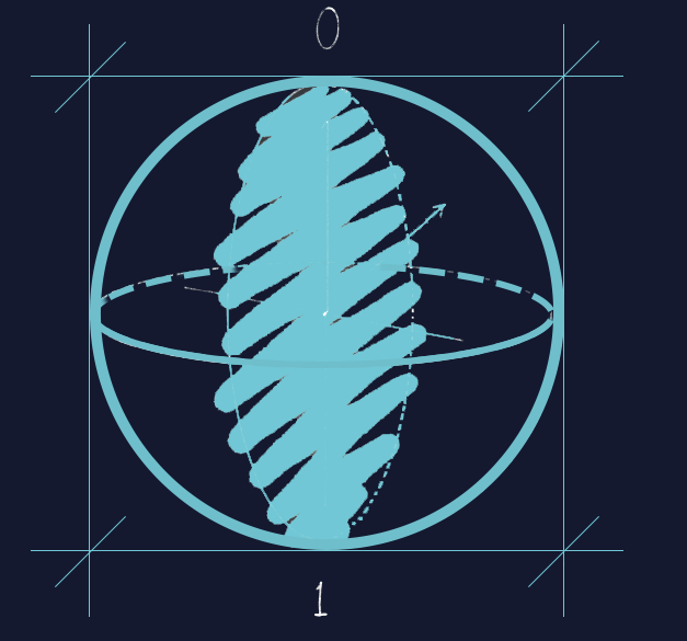
Gluon, g. In Feynman diagrams, emitted gluons are represented as helices. This diagram depicts the annihilation of an electron and positron. Source: Wikipedia
In addition to the strong nuclear force, there are three other fundamental forces in nature: electromagnetism, weak nuclear force, and gravity. Electromagnetism is responsible for interactions between charged particles, while weak nuclear force is responsible for certain types of radioactive decay. Gravity is responsible for the attraction between massive objects.
In particle physics, form factors are mathematical functions that describe how a particle interacts with other particles or fields. In the case of the proton, form factors can be used to describe how it interacts with electromagnetic fields (such as those produced by a photon) or gravitational fields (such as those produced by other massive objects).
The researchers in this study were specifically interested in determining the gluonic gravitational form factors of the proton. This refers to how gluons contribute to the gravitational mass of the proton. Gravitational mass is a measure of how much an object responds to a gravitational field - in other words, how much gravity it produces and how much gravity it feels from other objects. To investigate this phenomenon, the researchers used a small color dipole and threshold photoproduction of the J/ψ particle. A color dipole refers to two quarks that are separated by a distance - this creates an electric dipole moment that can interact with electromagnetic fields. The J/ψ particle is a type of meson that contains one charm quark and one charm anti-quark.
By using these tools, the researchers were able to investigate the gravitational density of gluons. They then analyzed their data using various models and were able to determine the gluonic gravitational form factors of the proton from their measurements.
One interesting finding from this study is that they determined a mass radius that is notably smaller than the electric charge radius. This means that there is more mass concentrated in a smaller volume than would be expected based on just looking at the electric charge distribution of the proton.
The researchers used a variety of models to analyze their data, including vector meson dominance (VMD), generalized vector dominance (GVD), and holographic QCD. VMD is a model that describes the interaction between photons and hadrons (particles made up of quarks and gluons). GVD is a more general version of VMD that includes additional mesons. Holographic QCD is a theoretical framework that uses string theory to describe the strong nuclear force.
In all cases, the researchers found that their determined mass radius was smaller than the electric charge radius. This suggests that there is more mass concentrated in a smaller volume than would be expected based on just looking at the electric charge distribution of the proton.
In some cases, depending on the model used, they found that their determined radius agrees well with first-principle predictions from lattice quantum chromodynamics (QCD). Lattice QCD is a computational technique used to study the strong nuclear force. It involves discretizing space-time into a lattice and using numerical simulations to calculate properties of particles such as quarks and gluons.
Overall, this research helps us better understand how gluons contribute to the gravitational mass of visible matter. It also has potential applications in fields such as nuclear physics and astrophysics, where understanding these properties can help us better model and predict phenomena such as neutron stars and black holes.
One interesting aspect of this study is that it highlights some of the challenges involved in studying subatomic particles. For example, because quarks are always confined within hadrons like protons, it can be difficult to directly measure their properties. Instead, researchers often have to rely on indirect methods like those used in this study.
Another challenge is that subatomic particles are subject to quantum mechanics, which means that their properties can be described by probability distributions rather than exact values. This can make it difficult to draw definitive conclusions from experimental data.
Required Additional Study Materials
- Particle Physics and Universe
- “An Introduction to Quantum Field Theory” by Michael E. Peskin and Daniel V. Schroeder
- “Quantum Chromodynamics” by Walter Greiner and Stefan Schramm
- “Gauge Theories in Particle Physics: A Practical Introduction” by Ian J.R. Aitchison and Anthony J.G. Hey
Reference
Duran, B., Meziani, ZE., Joosten, S. et al. Determining the gluonic gravitational form factors of the proton. Nature 615, 813–816 (2023).
Universal logic with encoded spin qubits in silicon
- Quantum Information
Fault tolerance is crucial for useful quantum hardware, requiring well-isolated qubits controlled with precision and high speed. Lithographically defined qubits, such as superconducting transmons or single electron spins in Si quantum dots, have made significant progress in scaling and control fidelity. However, achieving fault tolerance also depends on the structure and correlation of errors, which can be mitigated by using degenerate qubit states and coherent partial swap interactions. This alternative approach to quantum computation evokes classical conservative logic and allows for traversing the very large continuous special unitary group of $SU(2^n)$ for large n.
The researchers use a subsystem that encodes n/3 qubit states in n spins, with the remaining spins called leakage states. This allows for multi-qubit encoded universal quantum logic and avoids correlated errors. The partial swap operation needed for decoherence-free subspace (DFS) qubits is implemented using the contact exchange interaction between lithographically defined quantum dots, with a critical design difference being the removal of variation in spin splittings to maintain encoded-state degeneracy.
DFS qubit
These are a type of qubit that is designed to be less susceptible to decoherence, which is the loss of quantum information due to interactions with the environment. Decoherence is a major challenge in quantum computation, as it can cause errors and limit the performance of qubits. DFS qubits are designed to be more robust against certain types of environmental noise and can potentially enable more reliable quantum computation.
The device confines electrons in a silicon well with isotopic enhancement to reduce magnetic field gradients and control errors, and uses metallic gates to control interactions between electrons in quantum dots.
The SLEDGE platform allows for improved yield in the fabrication of quantum dots for practical EO operation in extended arrays. The SLEDGE architecture readily allows for extension of this geometry to 2d arrays by stacking via-connected routing layers, enabling 2d codes using high-fidelity native encoded-SWAP operation.
EO operation
EO operation refers to the energy-degenerate encoded qubit states controlled by nearest-neighbour contact interactions that partially swap the spin states of electrons with those of their neighbors, which is the alternative approach to quantum computation presented in the paper. The authors demonstrate this approach using silicon-based spin qubits and show that it is possible to perform universal logic operations with high fidelity. EO operation is different from traditional methods that rely on injecting microwave energy matching qubit resonances, which can lead to correlated errors and make achieving fault tolerance challenging.
Qubits are encoded using spins capable of partial swaps by associating quantum information with the total angular momentum quantum number of pairs of two spins. Addition of a third unmeasured spin to each qubit enables individual qubit control with only exchange, and no additional physical mechanism is needed to generate entanglement between these encoded qubits. Qubit preparation and measurement is achieved with Pauli spin blockade, which maps spin parity to the more easily detected charge configuration.
The researchers used baseband voltage pulses to control their encoded qubits through nearest-neighbor interactions. They achieved this by temporarily raising the exchange energy $J_{Xn}$ to $J_{Xn}/h \approx 100$ MHz using a single exchange pulse.
The researchers used FW-CNOT and SWAP gates for quantum computing and characterized their performance using quantum process tomography (QPT) and randomized benchmarking (RB). QPT showed qualitative agreement with expected results, but was limited by SPAM errors. RB was preferred as it was fast, simple, and relatively insensitive to SPAM error. The average two-qubit Clifford fidelity was 97.1% ± 0.2%, which was better than suggested by QPT and comparable to contemporary single silicon spin qubit two-qubit RB errors.
FW-CNOT gate
FW-CNOT is a type of controlled-NOT (CNOT) gate that is used in quantum computation. The “FW” in FW-CNOT stands for “flip-flop and wait”, which refers to the way the gate operates. The FW-CNOT gate is designed to flip the state of a target qubit if and only if the control qubit is in a specific state. This gate can be used as a building block for more complex quantum circuits and algorithms.
Quantum Process Tomography
Quantum process tomography (QPT) is a technique used to characterize the behavior of a quantum system. It involves applying a known set of input states to the system and measuring the corresponding output states. By analyzing the input-output relationship, it is possible to reconstruct the quantum process that describes how the system evolves over time. QPT can be used to identify errors and imperfections in a quantum system, which can help improve its performance and reliability.
Randomized Benchmarking
Randomized benchmarking (RB) is a method used to characterize the performance of quantum gates. It involves applying a randomly selected sequence of gates that compile to the identity from a discrete group of qubit operations, typically the Clifford group, to a quantum system. This choice depolarizes noise in the encoded subspace, allowing gate performance to be inferred by sweeping the sequence length and fitting return probability to an exponential decay. RB is fast, simple, relatively insensitive to SPAM error and requires measurement of only one qubit.
SPAM error
SPAM error refers to errors in state preparation and measurement (SPAM) that can occur in a quantum system. These errors can arise from imperfections in the hardware used to prepare and measure qubits, as well as from environmental noise and other sources of interference. SPAM errors can lead to incorrect measurements of the state of a qubit, which can in turn affect the performance of quantum gates and algorithms.
The performance of individual gates is measured using interleaved randomized benchmarking (iRB). iRB is performed for FW-CNOT and encoded SWAP, finding a fidelity of 96.3% ± 0.7% and 99.3% ± 0.5%, respectively. The SWAP error is more than five times lower than that of CNOT, making it a high-fidelity mechanism for moving data in constrained geometries. The dominant error in the EO operation is due to residual hyperfine interactions from the 800 ppm of 29Si nuclear spins and natural abundance of barrier 73Ge spins.
Interleaved Randomized Benchmarking
Interleaved randomized benchmarking (iRB) is a protocol used to measure the performance of individual gates in a quantum system. In iRB, the operation of interest is repeatedly interleaved between a random Clifford gate, and the resulting decay is compared with a reference RB decay to infer the operation’s fidelity. By comparing the decay rates of different gates, it is possible to identify which gates are performing well and which ones need improvement.
Researchers have successfully demonstrated encoded universal quantum logic operations using exchange-based partial swap interaction, which offers near-term opportunities for analogue simulation and potential for other computational modalities. Achieving fault tolerance with this method would require improved gate fidelity through faster control or improved isotopic purification.
Reference
Weinstein, A.J., Reed, M.D., Jones, A.M. et al. Universal logic with encoded spin qubits in silicon. Nature 615, 817–822 (2023).
Bright and stable perovskite light-emitting diodes in the near-infrared range
- Inorganic LEDs
Metal halide perovskites are a promising material for high-performance LEDs due to their outstanding properties. However, ensuring efficiency and stability at high brightness levels remains a hurdle for commercialization. A versatile molecule known as MSPE enhances the crystallinity, photoluminescence efficiency (the conversion of electrical energy to light), and minimizes Joule heating (the heat generated due to electrical resistance), resulting in effective and operationally stable near-infrared perovskite LEDs with high brightness.
Perovskite
Metal halide perovskites are a type of material that have a unique crystal structure, which allows them to exhibit exceptional optoelectronic properties. These materials are composed of a metal cation, a halide anion, and an organic cation. The combination of these components results in a crystal structure that is highly tunable and can be easily modified to achieve specific properties.
Perovskite LEDs based on the compound $\text{FAPbI}_3$ were developed using a layered device structure. The performance of the device depends on the ratio of MSPE to $\text{PbI}_2$. MSPE-based LEDs demonstrate a peak external quantum efficiency (EQE, the ratio of emitted photons to injected electrons) of 23.8% at a high radiance level of 39 W sr−1 m−2, outperforming some earlier perovskite, organic, and quantum-dot LEDs. These near-infrared emitters are suitable for various applications, such as imaging, optogenetics, night-vision, communication, and lasing.
MSPE devices showcase high energy conversion efficiency, reaching up to 16%. Pulsed voltages are employed to reduce Joule heating and extend the device’s lifespan. MSPE-based LEDs display good reproducibility and the best stability among perovskite LEDs. MSPE devices have an estimated $T_{50}$ (time to reach 50% of initial brightness) of 5 × 10^4 hours at an initial radiance of 5 W sr−1 m−2, comparable to state-of-the-art organic and quantum-dot LEDs.
The improved performance in MSPE-based devices is due to oriented crystallization and reduced disorder within the material. MSPE films exhibit increased photoluminescence quantum efficiency and less non-radiative recombination (when electron-hole pairs recombine without producing light). MSPE promotes denser, more regular island-shaped perovskite grains with better luminescence efficiency. MSPE reduces non-radiative recombination in perovskite grains, consistent with photoluminescence (PL) measurements.
Photoluminescence quantum efficiency
Photoluminescence quantum efficiency (PLQE) is a measure of the efficiency of a material to convert absorbed photons into emitted photons. It is defined as the ratio of the number of photons emitted by a material to the number of photons absorbed by that material. In other words, it represents the percentage of absorbed photons that are re-emitted as light. A higher PLQE indicates a more efficient conversion of absorbed energy into emitted light
Non-radiative recombination
Non-radiative recombination is a process in which an excited electron and hole pair in a material recombine without emitting a photon. In other words, the energy of the electron and hole is dissipated as heat or other non-radiative processes rather than being emitted as light.
In optoelectronic devices such as solar cells and LEDs, non-radiative recombination can be detrimental to device performance. This is because the energy lost through non-radiative recombination cannot be used to generate electrical power or light emission. Therefore, minimizing non-radiative recombination is important for improving device efficiency.
Non-radiative recombination can occur through various mechanisms, including defects in the material that trap charge carriers and prevent them from contributing to light emission or electrical power generation. These defects can arise from impurities, crystal lattice imperfections, or other factors that disrupt the ideal structure of the material.
Quantitative analysis of non-radiative recombination can be performed using techniques such as transient absorption measurements. By measuring the rate at which excited electrons and holes recombine through radiative and non-radiative processes, it is possible to evaluate the efficiency of a material for optoelectronic applications.
MSPE improves perovskite film quality by interacting with the compounds FAI and PbI2, slowing down growth and passivating unsaturated lead (Pb) dangling bonds, which can cause defects. MSPE can also interact with other MSPE molecules through hydrogen bonding between amino and sulfonyl groups, resulting in a more ordered structure. These interactions were confirmed through various spectroscopic techniques, such as FTIR, XPS, NMR, and DFT simulations.
Dangling bond
A dangling bond is an unsatisfied chemical bond on the surface of a material. It occurs when an atom on the surface of a material has fewer neighboring atoms than it would in the bulk of the material, leaving one or more unpaired electrons. These unpaired electrons can be highly reactive and can lead to unwanted chemical reactions or electronic properties.
MSPE molecules enhance perovskite film quality by reducing defects and disorder, leading to better photoluminescence quantum efficiency (PLQE) and carrier lifetime (how long an electron or hole exists before recombining). MSPE also serves as a physical spacer between charge-transport layers, preventing non-radiative energy loss at interfaces. Confocal PL microscopy and transient absorption measurements confirm the reduction of defect density in MSPE films compared to control films.
MSPE additives prevent the quenching (reduction) of luminescence in perovskites at charge-transport interfaces. Control devices show interfacial states with energies lower than the $\text{FAPbI}_3$ bandgap, leading to non-radiative energy loss. MSPE self-assembly between discontinuous perovskite grains eliminates these loss pathways in devices. Low-temperature solution-processable perovskite LEDs have the potential to achieve high efficiency at high brightness levels and surpass conventional LED technologies.
Required Additional Study Materials
- Fakharuddin, A., Gangishetty, M.K., Abdi-Jalebi, M. et al. Perovskite light-emitting diodes. Nat Electron 5, 203–216 (2022).
- Veldhuis, S.A., Boix, P.P., Yantara, N., Li, M., Sum, T.C., Mathews, N. and Mhaisalkar, S.G. (2016), Perovskite Materials for Light-Emitting Diodes and Lasers. Adv. Mater., 28: 6804-6834.
Reference
Sun, Y., Ge, L., Dai, L. et al. Bright and stable perovskite light-emitting diodes in the near-infrared range. Nature 615, 830–835 (2023).
Thousands of conductance levels in memrisistors integrated on CMOS
- Information Storage
Memristive devices have the potential to provide a virtually limitless number of conductance levels. However, fluctuations make it challenging to distinguish between these levels. By applying well-chosen electrical stimuli, we can control these fluctuations and achieve up to 2,048 distinct conductance levels. Incomplete conduction channels contribute to these fluctuations, but we can use denoising techniques to either strengthen or weaken them, which significantly enhances the memristor’s accuracy.
Memristor
A memristor is a type of electronic component that can “remember” the amount of charge that has flowed through it in the past. This means that its resistance can be changed by applying a voltage, and that change in resistance will persist even after the voltage is removed.
One of the key advantages of memristors is their ability to store information without using any power - this makes them very attractive for use in low-power devices like smartphones or Internet of Things (IoT) sensors. Additionally, because they can be used to perform both memory and computation functions, they have the potential to greatly improve the efficiency and speed of neural networks.
A commercial company fabricated memristors on an eight-inch wafer. To minimize fluctuations in the initial memristors, they applied small voltage pulses with carefully optimized amplitude and width. As a result, a single memristor reached 2,048 conductance states, ranging from 50 to $4,144 \mu S$, with a $2\mu S$ interval between adjacent states. The denoising process is crucial for training memristive neural networks, as unstable readings can lead to inaccurate outputs from the networks.
To achieve stable conductance states and memristive switching, it’s essential to study how conduction channels develop during electrical operations. C-AFM, a type of atomic force microscopy, was used to identify active conduction channels and remove incomplete channels, which ultimately denoises the device. These incomplete channels are more sensitive to voltage stimuli and can be adjusted without affecting complete channels.
Researchers investigated the denoising mechanism in memristors to determine if it was due to atomic or electronic effects. C-AFM scans consistently found incomplete channels when RTN (random telegraph noise) was observed, suggesting a connection between RTN and incomplete channels. The defects causing RTN might be oxygen atoms trapped between other atoms with large relaxation energies and long trapping or detrapping times. In memristors, RTN is mainly caused by electronic effects, not atomic ones.
RTN
RTN stands for Random Telegraph Noise, which is a type of noise that can occur in electronic devices. It is characterized by sudden, random changes in the current or voltage of a device, which can be caused by the trapping and release of individual charge carriers (like electrons) in defects within the device.
In the context of memristors, RTN can be a problem because it can cause fluctuations in the resistance of the device that are not related to any actual changes in the stored information. This can make it difficult to reliably read out the state of a memristor, particularly if there are many memristors operating together in a neural network.
Researchers have been studying RTN in memristors to better understand its causes and effects, and to develop strategies for mitigating its impact on device performance. Some studies have suggested that RTN may be induced by electronic effects rather than atomic effects, meaning that it may be related to changes in charge carrier density rather than physical movement of atoms within the device.
Blocking incomplete channels was modeled using C-AFM experiments and divided into three categories: non-conductive, conductive, and intermediate conductance. The Coulomb blockade mechanism, which describes how trapped charges can block electrical conduction, applies to nanoscale channels. Incomplete channels are easily blocked by trapped charges, making them the primary source of RTN. Denoising can be achieved by using a subthreshold voltage, which pushes the system towards equilibrium, reducing the high-energy boundary region and decreasing conductivity. Although the specific phases may vary for different materials, the approach and conclusions are broadly applicable.
Researchers successfully achieved 2,048 conductance levels in memristors and denoised them for high-precision operations. They then applied this process to an entire 256x256 crossbar array using on-chip driving circuitry. These findings offer valuable insights into memristive switching and represent significant progress towards commercializing memristor technology for machine learning and AI applications, making them more accessible to a broader audience.
Required Additional Study Materials
- “Handbook of Memristor Networks” by Chua, L., Sirakoulis, G. C., and Adamatzky, A.
Reference
Rao, M., Tang, H., Wu, J. et al. Thousands of conductance levels in memristors integrated on CMOS. Nature 615, 823–829 (2023).
Leave a comment