This review is written by non-expert and used for personal study only.
Distributed quantum sensing with mode-entangled spin-squeezed atomic states
- Quantum Metrology
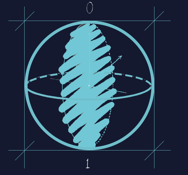
Distributed quantum sensors can accurately detect and compare phase shifts across spatially separated modes of quantum systems, making them ideal for network applications. Entanglement can enhance the precision of a spin-squeezed clock or sensor beyond the Quantum Projection Noise (QPN) limit. A mode-entangled system can potentially scale in accordance with the Heisenberg limit.
There are several approaches for generating spin-squeezing between spatially distinct modes, such as photonic Quantum Non-Demolition (QND) measurements, localized collisions in Bose-Einstein condensates, and atom-cavity interactions. Researchers have developed a network of atomic clocks with improved precision by entangling spins using velocity-dependent Raman transitions and spatially distributed QND measurements. The mode-entangled four-mode network exhibits significantly lower noise compared to equivalent mode-separable networks and networks of coherent spin states operating at the QPN limit.
To detect and squeeze the collective spin of numerous $^{87}$Rb atoms, researchers used QND measurements. Spatially separate modes were generated by employing velocity-dependent stimulated Raman transitions to link spin states to momentum $p$. The coherence between two modes is determined by applying a second Raman $\pi$ pulse and probing with a final microwave $\pi/2$ pulse.
By preparing ensembles of atoms in different initial states, researchers demonstrated the effect of phase shifts on each spatial mode. A microwave spin echo sequence was performed to adjust the phases of the microwave pulses and suppress phase noise. This property is advantageous for suppressing oscillator noise in clock comparisons and optical phase noise in light-pulse atom interferometry applications.
A sensor measuring differential phase shifts between two spatial modes can be utilized to measure frequency differences between two distant entangled clocks. Applying a magnetic field gradient across the separation between the two modes and introducing a clock frequency imbalance achieves this. The noise performance of entangled multimode clock networks can be quantified using a parameter derived from the generalized version of the Wineland squeezing parameter.
A two-mode SSS (spin-squeezed state) with squeezing reduces measurement variance, achieving precision comparable to a two-mode SSS without technical noise. Low measurement variance can be accomplished without high-performance local oscillators in a differential clock configuration. The method can be extended to a four-mode system with significant metrological enhancement.
The method detailed in the research paper was applied to an atom interferometer configuration. The interferometer pulse sequence involved a Raman $\pi$ pulse acting as a beamsplitter and a sequence of Raman $\pi$ pulse, microwave $\pi$ pulse, and Raman $\pi$ pulse acting as a mirror. The smallest observed single-shot phase uncertainty with a mode-entangled interferometer corresponded to an inferred differential acceleration sensitivity.
A distributed array of cavities with a common QND measurement and photonic links can enable entanglement and Bell tests across long distances. Adapting this method to squeezed optical clocks can push the limits of precision measurements of time and gravity. Applications in secure time transfer and quantum communications can benefit from a distributed entangled state. Additionally, the atomic interferometer protocol is useful for future high-performance gravity gradient sensors and differential configurations designed for gravitational wave detection and dark matter searches.
Required Additional Study Materials
- Zhang, Z. & Zhuang, Q. Distributed quantum sensing. Quantum Sci. Tech. 6, 043001 (2021).
Introductory material
- “Understanding Quantum Technologies 2022” by Olivier Ezratty
- “Quantum Sensing” by C. L. Degen, F. Reinhard, and P. Cappellaro
Reference
Malia, B.K., Wu, Y., Martínez-Rincón, J. et al. Distributed quantum sensing with mode-entangled spin-squeezed atomic states. Nature 612, 661–665 (2022).
Topological lattices realized in superconducting circuit optomechanics
- Quantum Metrology
Mechanical oscillators with ultra-low mechanical dissipation and compact form factors can be quantum controlled through coupling to electromagnetic cavities or superconducting qubits. This has enabled cooling to the ground state, state transfer, remote entanglement, and generation of squeezed mechanical states. Optomechanical lattices have the potential to access significantly richer and new dynamics, including topological phases of light and sound, collective and quench dynamics, quantum many-body dynamics, and entanglement. However, site-by-site engineerable optomechanical lattices have not yet been realized due to the stringent requirements on identical individual optomechanical sites.
Superconducting circuit optomechanical systems based on vacuum-gap capacitors have been used in a wide range of experiments, including the realization of optomechanical lattices with topologically protected edge states. These systems allow for direct measurement of collective microwave mode shapes and reconstruction of the full Hamiltonian, addressing an experimental challenge in large-scale multimode superconducting circuits.
The article discusses optomechanical lattices composed of optomechanical systems, where electromagnetic modes are mutually coupled with coupling rates $J_{ij}$. The Hamiltonian of such a lattice is described by a collective microwave mode basis, where each collective microwave mode is parametrically coupled to all the mechanical oscillators with the weight of the corresponding participation ratio. When the coupling strengths are designed to be alternating along a 1D chain, the microwave subsystem corresponds to a bosonic Su–Schrieffer–Heeger (SSH) chain, with two topologically distinct phases in between. The bulk-edge correspondence identifies the two phases by the winding number, which is topologically protected.
Implementing circuit optomechanical lattices is challenging due to low reproducibility of vacuum-gap capacitors. A nanofabrication process was developed to improve reproducibility and controllability of gap size. The process allows for control of microwave and mechanical resonance frequencies with fluctuations of less than 0.5% and 1%, respectively. The approach benefits from low mechanical dissipation.
Researchers fabricated a ten-site chain of LC resonators with alternating mutual inductive coupling to achieve a non-trivial topological phase and observed two topological edge modes in the middle of the bandgap. The microwave transmission spectrum of the chain was in good agreement with the calculated eigenfrequencies, indicating reliable control over the system parameters in the fabrication process.
The mechanical frequencies of each site were identified by incrementing the trench radius and measuring them using optomechanically induced transparency (OMIT), with ten OMIT features indicating mechanical frequencies matching the inverse trench radius relationship.
Researchers use mechanical oscillators to measure microwave mode shapes non-perturbatively. Optomechanical damping effect is used to deduce mode-shape information from mechanical oscillator dynamics. The effective damping rate of the mechanical mode is proportional to mode shape and can be measured experimentally. Mode-shape characterization on a ten-site chain shows excellent agreement with theoretical predictions, demonstrating bulk modes and topologically protected edge modes.
The Hamiltonian of the microwave subsystem can be reconstructed using eigenvectors and eigenvalues, and a unitary matrix obtained from measured participation ratios. The reconstructed Hamiltonian of the 1D SSH device shows cavity frequency disorder and alternating microwave couplings as designed for the SSH model, as well as parasitic second and third nearest-neighbour couplings between distanced sites.
The circuit optomechanical platform can be extended to 2D structures, as demonstrated by a 2D optomechanical honeycomb lattice. The coupling tunability is demonstrated by alternating mutual microwave couplings along the vertical axis, resulting in a phase transition and the emergence of edge modes. A 24-site circuit optomechanical system is designed on the border of the phase transition, realizing a strained graphene flake with edge states predicted using the bulk-edge correspondence. A full mode-shape measurement on the 2D lattice reveals close agreement with theoretical calculations, with four collective microwave modes localized in the two sites on either the top or bottom edges, as predicted by the topological analysis.
The study demonstrates optomechanical lattices with low disorder and direct measurement of the Hamiltonian, offering a path to explore physics in multimode optomechanics and generate highly entangled mechanical states.
In simpler terms, this research focuses on mechanical oscillators that are coupled to electromagnetic cavities or superconducting qubits, allowing for quantum control. Optomechanical lattices have the potential to exhibit new and interesting dynamics and entanglement. Researchers have been successful in creating a ten-site chain of LC resonators, which led to the observation of topological edge modes.
The mechanical frequencies of each site were identified using a technique called optomechanically induced transparency (OMIT). Mechanical oscillators were then used to measure microwave mode shapes non-perturbatively, with excellent agreement between experimental results and theoretical predictions.
The study successfully demonstrates the implementation of optomechanical lattices with low disorder and the ability to directly measure the Hamiltonian. This opens up the possibility to explore new physics in multimode optomechanics and generate highly entangled mechanical states, which may have significant implications for the future of quantum technologies.
Required Additional Study Materials
- Aspelmeyer, M., Kippenberg, T. J. & Marquardt, F. Cavity optomechanics. Rev. Mod. Phys. 86, 1391 (2014).
- Carusotto, I. et al. Photonic materials in circuit quantum electrodynamics. Nat. Phys. 16, 268–279 (2020).
- Asbóth, J. K., Oroszlány, L. & Pályi, A. A Short Course on Topological Insulators. Lecture Notes in Physics Vol. 919, 997 (Springer, 2016).
- Ozawa, T. et al. Topological photonics. Rev. Mod. Phys. 91, 015006 (2019).
- Naumis, G. G., Barraza-Lopez, S., Oliva-Leyva, M. & Terrones, H. Electronic and optical properties of strained graphene and other strained 2d materials: a review. Rep. Prog. Phys. 80, 096501 (2017).
- Surjadi, J. U. et al. Mechanical metamaterials and their engineering applications. Adv. Eng. Mater. 21, 1800864 (2019).
Introductory material
- “Superconducting Circuit Companion—an Introduction with Worked Examples” by S.E. Rasmussen et al.
- “Shortcut to Superconductivity: Superconducting Electronics via COMSOL Modeling” by Armen Gulian
Reference
Youssefi, A., Kono, S., Bancora, A. et al. Topological lattices realized in superconducting circuit optomechanics. Nature 612, 666–672 (2022).
A membrane-based seawater electrolyser for hydrogen generation
- Hydrogen Energy
Electrolysis is a process that uses electricity to split water molecules into hydrogen and oxygen gases. However, conventional methods of seawater electrolysis cause electrocatalyst corrosion and failure within a short amount of time.
To address this issue, a new strategy has been developed that uses a self-driven phase transition mechanism to purify seawater in situ for electrolysis. This strategy involves using a hydrophobic porous polytetrafluoroethylene (PTFE)-based waterproof breathable membrane as a gas-path interface and a concentrated potassium hydroxide (KOH) solution as a self-dampening electrolyte (SDE).
The design of this strategy allows for the generation of pure water for electrolysis from seawater with 100% ion-blocking efficiency, resulting in sustainable hydrogen (H2) generation. This is because the hydrophobic PTFE membrane is able to prevent liquid penetration while allowing for directional water vapor transport, enabling stable ion concentrations in the SDE for a longer period of time.
Furthermore, the energy expense of H2 production using this strategy is comparable to that of industrial alkaline electrolysis with pure water, thanks to the elimination of a separate desalination process. This makes the strategy an attractive option for sustainable H2 production.
The self-dampening electrolyte (SDE) is a key component of this strategy. It possesses specific properties that enhance water migration from seawater to the SDE without extra energy consumption. The KOH solution used as the SDE exhibits SDE-like functions and undergoes four stages in the self-dampening process. The optimal SDE concentration is 30 wt% KOH, which has the highest conductivity and creates a reasonable difference in water vapor pressure from that of seawater.
A simulation using an ideal porous gas-path system with seawater and an SDE has provided insights into the water migration process. The simulations predict the water migration potential at different depths and temperatures, expanding the adaptability of this approach. The feasibility of deep-ocean H2 generation using this water phase transition migration strategy has been demonstrated, and the scalable system holds great promise for energy construction of ecological floating islands due to its compact design and exceptional performance.
This direct seawater splitting approach employs a self-breathable waterproof membrane and a solid hygroscopic SDE, demonstrating superior electrolysis performance using a PVA/KOH hydrogel and a synthesized Mo-Ni3S2/NF electrocatalyst. The strategy is applicable to other non-volatile liquids and may be used for simultaneous H2 production and recovery of useful resources.
Overall, this approach to seawater electrolysis offers several advantages over traditional methods, including greater efficiency, reduced energy consumption, and improved sustainability. It holds great promise for the future of renewable energy production.
Required Additional Study Materials
- Tong, W. et al. Electrolysis of low-grade and saline surface water. Nat. Energy 5, 367–377 (2020).
- Jones, E., Qadir, M., van Vliet, M. T., Smakhtin, V. & Kang, S.-M. The state of desalination and brine production: a global outlook. Sci. Total. Environ. 657, 1343–1356 (2019).
- Yang, K. et al. A roadmap to sorption-based atmospheric water harvesting: from molecular sorption mechanism to sorbent design and system optimization. Environ. Sci. Technol. 55, 6542–6560 (2021).
- Tereshchenko, & Anatoly, G. Deliquescence: hygroscopicity of water‐soluble crystalline solids. J. Pharm. Sci. 104, 3639–3652 (2015).
Introductory material
- “Seawater electrolysis for hydrogen production: a solution looking for a problem?” by M. A. Khan et al.
- “Progress in theoretical and experimental investigation on seawater electrolysis” by X. Zhang et al.
Reference
Xie, H., Zhao, Z., Liu, T. et al. A membrane-based seawater electrolyser for hydrogen generation. Nature 612, 673–678 (2022).
Synthesis-on-substrate of quantum dot solids
- Quantum Dots
Synthesizing blue perovskite emitters is a challenging task due to the segregation of halides and difficulties in achieving monodispersed sub-5 nm-sized quantum dots (QDs) via traditional colloidal synthesis methods. Moreover, the coupling of ligands during film formation is particularly challenging for ultraconfined dots, which results in redshift and increased emission linewidth. However, one potential solution is to combine synthesis and film fabrication into a single step.
To ensure inter-dot coupling, compact and conjugated ligands are necessary, along with preventing layered perovskite precipitation and strong ligand surface binding affinity. Researchers used conventional PEA+ ligands as a starting point and prepared perovskite films via single-step spin-coating and antisolvent dripping. However, they observed layered perovskites in both grazing-incidence wide-angle X-ray scattering (GIWAXS) patterns and transient absorption spectra.
To prevent the formation of layered perovskites, researchers used sterically hindered ligands that create severe octahedral distortion. Adding an extra methyl substitution to the head group of the ligand resulted in the formation of only cubic CsPbBr3 and CsPbI3 perovskites. Films using MBA+ ligands emitted at a wavelength corresponding to bulk CsPbBr3. Halide substitution was pursued to increase the surface binding affinity of the ligand, and α-methyl-4-bromide-benzylammonium (Br-MBA+) was synthesized with bromide substitution at the para position of the tail group. Continuous tuning of photoluminescence wavelength was achieved with Br-MBA+ films, distinguishing them from 2D and quasi-2D layered perovskites.
GIWAXS and X-ray diffraction (XRD) measurements show the CsPbBr3 phase in QDs with varying diameters and a blue shift in photoluminescence due to increased ligand concentration. In situ GIWAXS reveals three distinct stages of CsPbBr3 QD formation, including a metastable intermediate phase, which contributes to a narrow size distribution. In situ photoluminescence spectra were used to study bandgap evolution during film growth of QDs. Ligand concentration and binding affinity play key roles in the crystallization process during solid-state synthesis, allowing for tunable QD size production. The tail group of the ligands influences surface binding affinity, with high binding energy and low adsorption barrier facilitating strongly confined QD formation. F-MBA+ ligands display a higher adsorption barrier compared to other ligands, making it challenging to adsorb multiple F-MBA+ ligands on the CsPbBr3 surface.
Extracting the exciton binding energy (Exb) of perovskites from photoluminescence measurements may overestimate the value due to the possibility of structural transition at low temperatures. Blue QD films exhibit decreased effective photoluminescence lifetime and strong first-order exciton recombination, with a photoluminescence quantum yield of 80% and FWHM ≈ 23 nm. The QD films have a low defect density and trap state density (ηtrap) of $10^{15} cm^{−3}$, with a hole mobility of $μ = 3 × 10^{−3} cm^{2} V^{−1} s^{−1}$ and similar conductivity (σ) to conventional CsPbBr3 films. CsPbBr3 QD film samples retain a photoluminescence quantum yield above 90% over 60 min at 80 °C, indicating good thermal stability compared to control CsPbBr3 films.
Researchers have fabricated primary blue PeLEDs using QD films with the highest reported external quantum efficiency (EQE) of 12.3%. The LED performance showed a maximum EQE of 17.9% with the electroluminescence peak at 480 nm and a FWHM of approximately 21 nm. This is a significant improvement in primary blue PeLEDs, with an EQE that is 1.5 times higher than previous reports. Additionally, the operating half-lifetime ($T_{50}$) at an initial luminance of $100 cd m^{−2}$ is 2 hours, which is approximately 5 times higher than the best reported efficient blue PeLEDs.
The researchers also fabricated deep-blue PeLEDs with CsPbBr3 QDs of about 3.5 nm, achieving an EQE of 10.3% with an electroluminescence peak at 465 nm and a FWHM of 23 nm. This EQE is also a significant improvement compared to previous perovskites in similar wavelengths, indicating the versatility and potential of these QDs for use in various applications.
Overall, these findings suggest that using sterically hindered ligands can effectively prevent the formation of layered perovskites and produce high-quality CsPbBr3 QDs for use in PeLEDs with improved efficiency and stability. This approach provides insights into the factors that affect the synthesis of blue perovskite emitters and paves the way for further developments in the field of perovskite-based optoelectronics.
Required Additional Study Materials
- Liu, X. et al. Metal halide perovskites for light-emitting diodes. Nat. Mater. 20, 10–21 (2021).
- Akkerman, Q. A., Raino, G., Kolalenko, M. V. & Manna, L. Genesis, challenges and opportunities for colloidal lead halide perovskite nanocrystals. Nat. Mater. 17, 394–405 (2018).
- Kovalenko, M. V., Protesescu, L. & Bodnarchuk, M. I. Properties and potential optoelectronic applications of lead halide perovskite nanocrystals. Science 358, 745–750 (2017).
- Li, X., Hoffman, J. M. & Kanatzidis, M. G. The 2D halide perovskite rulebook: how the spacer influences everything from the structure to optoelectronic device efficiency. Chem. Rev. 121, 2230–2291 (2021).
- Xue, J., Wang, R. & Yang, Y. The surface of halide perovskites from nano to bulk. Nat. Rev. Mater. 5, 809–827 (2020).
- Blancon, J., Een, J., Stoumpos, C. C., Kanatzidis, M. G. & Mohite, A. D. Semiconductor physics of organic–inorganic 2D halide perovskites. Nat. Nanotechnol. 15, 969–985 (2020).
- deQuilettes, D. W. et al. Charge-carrier recombination in halide perovskites. Chem. Rev. 119, 11007–11019 (2019).
Introductory material
- “Quantum Dots” edited by Alexander Tartakovskii
- “Quantum Dots - Fundamental and Applications” edited by Faten Divsar
Reference
Xie, H., Zhao, Z., Liu, T. et al. A membrane-based seawater electrolyser for hydrogen generation. Nature 612, 673–678 (2022).
Additive manufacturing of micro-architected metals via hydrogel infusion
- Metals and Alloys
Metal additive manufacturing (AM) is typically achieved using either powder bed fusion or directed energy deposition techniques. However, vat photopolymerization (VP) using digital light processing (DLP) printing offers a promising alternative for shaping parts with high print speeds and submicrometer resolution. While the inorganic material selection for VP remains limited, researchers have demonstrated the ability to fabricate nanoscale silver and nickel using hydrogels and inorganic-organic resins.
To overcome the limitation of material selection for VP, a new additive manufacturing technique has been developed, called hydrogel infusion additive manufacturing (HIAM). HIAM uses 3D architected hydrogel scaffolds as platforms for subsequent in situ material synthesis reactions to fabricate a wide range of micro-architected metals and alloys. The process involves DLP printing, solvent exchange, metal salt precursor solution soaking, calcination, and reduction in forming gas to yield metal or alloy replicas of the designed architecture. This approach allows for parallelization of printing and material selection, enabling exploration of a larger compositional space, including multimaterials, which is not possible with existing VP methods.
The metal microlattices produced through HIAM were characterized using scanning electron microscopy (SEM) and focused ion beam (FIB) milling, revealing dense and relatively defect-free structures with a homogenous distribution of copper (Cu) and nickel (Ni) in the CuNi lattice. The chemical composition of the microlattices was investigated using X-ray diffraction (XRD), energy-dispersive X-ray spectroscopy (EDS), thermogravimetric analysis (TGA), and differential scanning calorimetry (DSC). The Cu and CuNi microlattices contained 93% and 86% of the target materials, respectively, with the remainder being carbon and aluminosilicate contamination. Calcination and reduction of the metal-nitrate-infused gels produced metal oxide replicas that were converted to Cu and a homogenous CuNi alloy, respectively. During calcination, the Cu and CuNi precursor gels retained 12.7% and 15.8% of their original mass, respectively, and reached mass stabilization between 370°C and 380°C. Both Cu and CuNi gels exhibited similar normalized heat flow profiles with exothermic peaks beginning at approximately 235°C and reaching a maximum heat flow of -1.5 W g$^{-1}$ for Cu and -2.6 W g$^{-1}$ for CuNi at 304°C.
Transmission electron microscopy (TEM) analysis of Cu fabricated through HIAM showed well-formed grain and twin boundaries without voids, but with aluminosilicate inclusions resulting from furnace tube contamination. Cu had an area-weighted average grain size of 13.74 ± 8.43 μm, and CuNi had an area-weighted average grain size of 9.81 ± 4.79 μm. Nanoindentation experiments on HIAM-fabricated Cu and CuNi showed their respective hardness values to be 1.81 ± 0.37 GPa and 2.15 ± 0.22 GPa, with twin boundaries increasing measured hardness. A modified Hall-Petch relation was introduced to account for the effect of twin boundaries on dislocation motion during deformation.
Calcination of the Cu and CuNi precursors involved multiple thermally induced processes, including dehydration, thermal decomposition, and combustion reactions. Both Cu and CuNi precursor gels exhibited exothermic events around 300°C attributed to the combustion of the PEGda polymer scaffold and oxidation of the metal ions. The CuNi gel released heat more rapidly than the Cu gel, and the nickel nitrate salt contributed to the oxidation reaction at a lower temperature. The presence of defects and pores was correlated with higher maximum dW/dT, and slowing the rate of mass loss during calcination increased the HIAM part density.
The high annealing twin densities observed in HIAM metals did not fully explain the increase in hardness, which is likely due to atomic-scale features formed during the HIAM process, such as dissolved carbon.
A significant advantage of HIAM is its ability to allow material selection after part shaping, simplifying the material development process and enabling the fabrication of complex materials and multimaterial metal structures. In traditional AM processes, material selection is done before part shaping, making the feedstock inseparable from the final material composition. HIAM’s approach opens up new opportunities for the fabrication of energy materials, micro-electromechanical systems, and biomedical devices using a versatile VP approach that can create micro-architected metal 3D structures.
Moreover, HIAM enables the fabrication of metallic multimaterials and multicomponent alloys with superior high-temperature behavior and enhanced yield strength, making it a practical and powerful capability for industrial use. HIAM’s generalizability to other gel-producing AM processes, such as direct ink writing and two-photon lithography, adds to its value as a versatile and promising additive manufacturing technique.
HIAM represents an innovative approach to fabricating complex materials and structures with a high degree of accuracy, speed, and versatility. It enables material selection after part shaping, opening up new possibilities for the development of a wide range of micro-architected metals and alloys with advanced properties. With its ability to fabricate metallic multimaterials and multicomponent alloys, HIAM holds significant potential for industrial use in a variety of applications, including energy materials, micro-electromechanical systems, and biomedical devices.
Required Additional Study Materials
- Vafadar, A., Guzzomi, F., Rassau, A. & Hayward, K. Advances in metal additive manufacturing: a review of common processes, industrial applications, and current challenges. Appl. Sci. 11, 1213 (2021).
- Mohd Yusuf, S., Cutler, S. & Gao, N. Review: the impact of Mmtal additive manufacturing on the aerospace industry. Metals 9, 1286 (2019).
- Velásquez-García, L. F. & Kornbluth, Y. Biomedical applications of metal 3D printing. Annu. Rev. Biomed. Eng. 23, 307–338 (2021).
- Plocher, J. & Panesar, A. Review on design and structural optimisation in additive manufacturing: towards next-generation lightweight structures. Mater. Des. 183, 108164 (2019).
- Bartlett, J. L. & Li, X. An overview of residual stresses in metal powder bed fusion. Addit. Manuf. 27, 131–149 (2019).
- Zhang, D., Liu, X. & Qiu, J. 3D printing of glass by additive manufacturing techniques: a review. Front. Optoelectron. 14, 263–277 (2021).
- Chen, Z. et al. 3D printing of ceramics: a review. J. Eur. Ceram. Soc. 39, 661–687 (2019).
- Yee, D. W. & Greer, J. R. Three-dimensional chemical reactors: in situ materials synthesis to advance vat photopolymerization. Polym. Int. 70, 964–976 (2021).
- Dass, A. & Moridi, A. State of the art in directed energy deposition: from additive manufacturing to materials design. Coatings 9, 418 (2019).
- Li, Y. et al. A review on functionally graded materials and structures via additive manufacturing: from multi-scale design to versatile functional properties. Adv. Mater. Technol. 5, 1900981 (2020).
- Kajtaz, M., Subic, A., Brandt, M. & Leary, M. in Materials in Sports Equipment (ed. Subic, A.) 161–198 (Elsevier, 2019).
- Zhang, B. et al. Highly stretchable hydrogels for UV curing based high-resolution multimaterial 3D printing. J. Mater. Chem. B 6, 3246–3253 (2018).
- Gun’ko, V. M., Savina, I. N. & Mikhalovsky, S. V. Properties of water bound in hydrogels. Gels 3, 37 (2017).
- Danks, A. E., Hall, S. R. & Schnepp, Z. The evolution of ‘sol–gel’ chemistry as a technique for materials synthesis. Mater. Horiz. 3, 91–112 (2016).
- Moore, J. J. & Feng, H. J. Combustion synthesis of advanced materials: part I. Reaction parameters. Prog. Mater. Sci. 39, 243–273 (1995).
- Senkov, O. N., Miracle, D. B., Chaput, K. J. & Couzinie, J. P. Development and exploration of refractory high entropy alloys - A review. J. Mater. Res. 33, 3092–3128 (2018).
Introductory material
- “Additive Manufacturing Technologies” by Ian Gibson, David Rosen, Brent Stucker, and Mahyar Khorasani
- “Advances in Understanding Hydrogel Lubrication” by Tooba Shoaib and Rosa M. Espinosa-Marzal
Reference
Saccone, M.A., Gallivan, R.A., Narita, K. et al. Additive manufacturing of micro-architected metals via hydrogel infusion. Nature 612, 685–690 (2022).
Condensed-phase isomerization through tunnelling gateways
- Reactin Kinetics and Dynamics
Tunnelling is a phenomenon in which particles penetrate through an energy barrier that they do not possess enough energy to surmount classically. It can be a dominant factor in important chemical reactions, including those occurring in cold interstellar clouds and enzyme reactions. Tunnelling rates can become nearly temperature-independent in the “deep-tunnelling regime,” which reflects tunnelling from the ground state of the reactant. Kinetic isotope effects (KIEs) can be used to identify tunnelling, with the largest KIEs found for H-substitution by deuterium or tritium.
To better understand condensed-phase tunnelling, researchers seek a simpler model system and first-principles theory. They used a simple isomerization reaction on a $NaCl$(100) surface as a model system for comparison of experiment to theory. Infrared absorption spectroscopy was used to obtain measurements of thermal tunnelling rates for the conversion of O-bound to C-bound CO in buried monolayers of isotopologues, and a quantum rate theory for condensed-phase tunnelling was presented.
The researchers found that the isomerization rates of CO isotopologues on an $NaCl$(100) surface show a nonmonotonic mass dependence, with $^{13}C^{16}O$ reacting most rapidly, followed by $^{12}C^{16}O$, then $^{13}C^{18}O$. The temperature-dependent rate constants for all three isotopologues show nonmonotonic mass dependence, with $^{13}C^{18}O$ approaching the rates of $^{13}C^{16}O$ as temperature increases, suggesting that the rates for $^{13}C^{18}O$ might exceed those of both lighter isotopologues above 24 K.
The Arrhenius parameters suggest that the rate constants reflect a tunnelling process. The concept of tunnelling gateways is introduced to explain observations in CO rotational isomerization, including nonmonotonic mass dependence and small derived values of $A_{obs}$ relative to $A^{TST}$. The gateway concept explains erratic mass dependence and T dependence in isotopologues by providing an intuitive understanding of Arrhenius parameters through energy shifts and tunnelling probability.
To test the gateway hypothesis, researchers developed a quantum rate theory using the Schrödinger equation to obtain vibrational eigenstates and compute thermal rates for population transfer between localized states. The FGR model captured some experimental observations, showing a strong mass dependence in the Arrhenius parameters and a range of temperatures where heavier isotopologues tunnel faster than lighter ones.
The FGR model predicts an unexpected KIE in the deep-tunnelling regime, where the FGR rate constants are nearly temperature-independent. The presented model aims to give a qualitative explanation for a nonmonotonic mass dependence of tunnelling rates and provides a more rigorous basis for tunnelling gateways. However, the FGR model does not perfectly reproduce experimental data due to the accidental nature of tunnelling gateways and the simplicity of the model.
This research suggests that interstellar chemistry may involve tunnelling reactions in ices on dust grains, which current models may overlook due to the importance of quantum gateways not being recognized. It also reveals that condensed-phase tunnelling occurs when environmental interactions induce transitions between bound states localized across the reaction barrier, compensated for by exchange of phonons. This model could be extended to other systems and explain the KIEs of previous work on CO binding to myoglobin.
Required Additional Study Materials
- Klinman, J. P. & Kohen, A. Hydrogen tunneling links protein dynamics to enzyme catalysis. Annu. Rev. Biochem. 82, 471–496 (2013).
Introductory material
- “Quantum Tunneling in Condensed Media” edited by Yu. Kagan and A.J. Leggett
- “Tunneling Systems in Amorphous and Crystalline Solids” edited by P. Esquinazi
Reference
Choudhury, A., DeVine, J.A., Sinha, S. et al. Condensed-phase isomerization through tunnelling gateways. Nature 612, 691–695 (2022).
Leave a comment