This review is written by non-expert and used for personal study only.
Formation of robust bound states of interacting microwave photons
- Quantum Information
Photons usually don’t interact in a vacuum. However, superconducting circuits create a structure that allows photons to interact and create coherent bound states, or groups of photons that act together. Quantum processors, which use special gates called unitary gates, make it possible for these bound states to form within complex dynamics called Floquet systems.
Integrable models are essential for understanding how different systems in physics behave over time, and they help us test quantum processors. The XXZ model is an example of a model that allows bound states to form. Quantum processors are particularly useful for studying these models when traditional mathematical methods are not efficient.
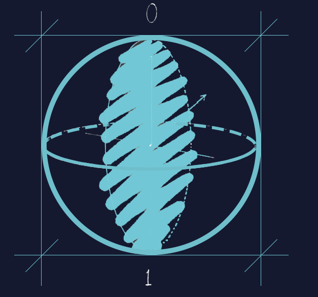
Bound states appear when certain conditions are met in the system, represented by a combination of bitstrings (strings of 0s and 1s). In Floquet systems, bound states are difficult to form since these systems don’t have a clear lowest energy state. However, interactions between photons can help balance out the energy and make it possible for bound states to form. In the experiment, researchers used a specific sequence to control a chain of $24$ qubits study this phenomenon.
To understand how bound photons stay together, researchers measured the photon occupancy at neighboring locations. The presence of two wavefronts for a certain photon number ($n_{ph}=2$) indicates that a two-photon bound state exists. They also found that the velocities of these wavefronts matched theoretical predictions. The slow decay of bitstrings with adjacent photons was due to disturbances in the system and the breaking of connections at the bound state’s edges.
Using a technique called many-body spectroscopy, researchers found that bound photons have well-defined properties like momentum, energy, and charge, which make them quasiparticles. They measured the energy of these bound states by comparing how their phase changed over time relative to a reference state. This method relied on measuring a property called the Green’s function of the system. This analysis showed that the structure of single-particle and many-body states changes as more photons and interaction energy are introduced. A bound state was also observed in a weakly interacting system due to the interference between the decay products of the bound state.
External magnetic fields can help identify a property called electric pseudo-charge in quasiparticles by shifting their energy bands. Researchers created a synthetic magnetic field by rotating qubits, which caused a shift in the momentum of observed states with the correct pseudo-charge. The experiment confirmed a theoretical prediction that bound states within a continuum exist due to the periodic nature of a property called quasi-energy.
Researchers also investigated how bound states are affected when the underlying symmetry of the system is disrupted. They found that small disruptions lead to rapid decay of the bound states, while a specific bound state ($n_{ph}=3$) was resistant to much larger disruptions. Spectroscopy techniques confirmed the presence of these resilient bound states.
Usually, non-integrable disruptions cause bound states to decay, but this experiment found that they can be more resilient than expected. This might be due to the relationship between integrability and a phenomenon called prethermalization. The experiment was made possible by high-quality quantum gates and the ability to directly measure complex relationships in the system. This allowed researchers to observe the formation of bound states involving multiple photons and uncover their resilience to non-integrable disruptions.
Required Additional Study Materials
- Eckle, H. P. Models of Quantum Matter: A First Course on Integrability and the Bethe Ansatz (Oxford Univ. Press, 2019).
- Greene, C. H., Giannakeas, P. & Pérez-Ríos, J. Universal few-body physics and cluster formation. Rev. Mod. Phys. 89, 035006 (2017).
- Chang, D., Vuletic, V. & Lukin, M. Quantum nonlinear optics—photon by photon. Nat. Photon. 8, 685–694 (2014).
- Blatt, R. & Roos, C. F. Quantum simulations with trapped ions. Nat. Phys. 8, 277–284 (2012).
- Gross, C. & Bloch, I. Quantum simulations with ultracold atoms in optical lattices. Science 357, 995–1001 (2017).
- Carusotto, I. et al. Photonic materials in circuit quantum electrodynamics. Nat. Phys. 16, 268–279 (2020).
- Hsu, C. W., Zhen, B., Stone, A. D., Joannopoulos, J. D. & Soljacic, M. Bound states in the continuum. Nat. Rev. Mater. 1, 16048 (2016).
Introductory material
- “Quantum Information and Quantum Optics with Superconducting Circuits” by Juan José García Ripoll
- “A Textbook on Modern Quantum Mechanics” by A C Sharma
Reference
Morvan, A., Andersen, T.I., Mi, X. et al. Formation of robust bound states of interacting microwave photons. Nature 612, 240–245 (2022).
Spin-orbit microlaswer emitting in a four-dimensional Hilbert space
- Quantum Optics
Information systems traditionally use binary digits, but quantum bits (qubits) offer more possibilities by allowing superpositions, which increases information density and security. Optical beams, which have properties called spin and orbital angular momentum, can help create high-dimensional spaces called Hilbert spaces, which can improve communication network efficiency. Manipulating these properties of light can lead to a 4D Hilbert space, but previously, the progress has been limited.
A new semiconductor microlaser, which uses the spin-orbit coupling of light, allows control over multiple aspects (six degrees of freedom) and full access to a 4D Hilbert space. This laser can generate and reconfigure high-dimensional superposition states, which are combinations of quantum states, by mapping them onto a Bloch hypersphere defined by a mathematical structure called $SU(4)$ algebra.
The hyperdimensional microlaser emits light in a 4D Hilbert space and consists of two microrings connected through control waveguides. Each microring supports two degenerate modes, forming a mathematical structure called an $SU(2)$ group, and the entire laser functions as a four-level system. The microlaser has four degrees of freedom for controlling two $SU(2)$ groups and two additional degrees of freedom to realize a full 4D Hilbert space. The microlaser features three high-order Poincaré spheres (HOPSs) with a total of six degrees of freedom, representing an $ SU(4)$ symmetry in a 4D Hilbert space.
Researchers use HOPS I and HOPS II to represent the left and right rings, with carefully designed microring cavities. The four spin-orbit-coupled states fully overlap in space and time, sharing the same properties and enabling coherence after long-distance propagation. HOPS III completes the $SU(4)$ hypersphere, with its north and south pole states arbitrarily chosen from HOPS II and HOPS I, respectively. Full control over the six degrees of freedom involves a representation of the $SU(4)$ group.
The system allows independent control of the three HOPSs, with HOPS I and HOPS II selectively characterized and manipulated. Heating pads and optical pumping techniques control gain and phase accumulation, which are essential for laser operation. The system also enables $SU(4)$ state control on HOPS III by adjusting two degrees of freedom between the microrings.
Researchers explain the control of the $SU(4)$ Bloch hypersphere using vectorial states on HOPS III. The gain/loss contrast and phase tuning between two microrings can be controlled using specific parameters in an equation. Phase control between the microrings is achieved with a technique called on-site frequency detuning. This ability to map vectorial states on the $SU(4)$ Bloch hypersphere allows the generation and reconfiguration of high-dimensional states that are resistant to noise, which is essential for error correction in computations and communications.
The developed spin-orbit micro-laser can generate and reconfigure high-dimensional superposition states with high fidelity, making it suitable for secure communication methods like quantum key distribution and precision metrology. This hyperdimensional microlaser offers an integrated solution for next-generation high-capacity, noise-resistant communication technologies.
Required Additional Study Materials
- Wang, Y., Hu, Z., Sanders, B. C. & Kais, S. Qudits and high-dimensional quantum computing. Front. Phys. 8, 589504 (2020).
Introductory material
- “Quantum Optics and Quantum Computation: An introduction” by Dipankar Bhattacharyya and Jyotirmoy Guha
- “Quantum Mechanics: A Textbook” by Arjun Berera and Luigi Del Debbio
- “Fundamentals of Quantum Optics and Quantum Information” by Peter Lambropoulos and David Petrosyan
Reference
Zhang, Z., Zhao, H., Wu, S. et al. Spin–orbit microlaser emitting in a four-dimensional Hilbert space. Nature 612, 246–251 (2022).
Integrated femtosecond pulse generator on thin-film lithium niobate
- Nanoscale Devices
Creating extremely short, broad-spectrum, and high-power optical pulses on a chip has been a long-standing goal in the field of optics. Current demonstrations rely on bulky table-top pulse laser sources, which are not practical for everyday applications. Electro-optic comb generators offer a more flexible and efficient alternative for producing optical pulses. An electro-optic time lens system can compress continuous-wave light into a short pulse, with the shortest possible pulse width determined by the phase modulator’s voltage and the microwave voltage applied to it.
Previously, systems required multiple phase modulators and an intensity modulator to achieve the necessary optical bandwidth for picosecond pulses, which led to high complexity and cost. To address these limitations, researchers have integrated an electro-optic comb source on a lithium niobate photonic chip. This chip features low-loss nanophotonic waveguides and excellent electro-optic efficiency. The chip combines an amplitude modulator, a phase modulator, and a dispersive waveguide, along with spot-size converters for efficient light coupling. The new phase modulator design reduces a critical voltage value ($V_{\pi}$) by half, with an electro-optic bandwidth of $45 GHz$ and a $V_π$ of $2-2.5 V$ in the $4-39 GHz$ radio-frequency range.
Compared to traditional setups, the time-lens chip generates ultrafast pulses with lower power consumption and less complex control circuitry. The chip achieves impressive modulation indices, resulting in extremely short pulses after compression in a standard optical fiber. The integrated time-lens platform enables optical frequency comb generation with microwave line spacings, offering benefits such as frequency adaptability, robust operation, and improved comb efficiency.
Researchers demonstrated nonlinear frequency conversion by using time-lens pulses to pump a highly nonlinear fiber. This pulse source can directly link optical and microwave domains for self-referencing and can help address challenges in bandwidth and line-number products. By replacing the optical fiber with a specially designed waveguide for on-chip compression, a fully integrated ultrafast source can be achieved. However, the current propagation loss of the waveguide limits the usable length, resulting in an on-chip pulse duration of 8 picoseconds.
An integrated chirped Bragg grating in lithium niobate can be used for dispersion management and pulse compression. This grating exhibits low propagation loss, high reflectivity, and better dispersion properties compared to optical fibers. Researchers integrated a $1.75$-mm-long chirped grating with the rest of the time lens on the same chip to demonstrate a fully integrated ultrafast pulse source. The chip was fabricated using a wafer-scale process, but faced a trade-off between resolution and chip size, leading to a significant on-chip insertion loss.
Researchers have developed an electro-optic comb generator on a photonic chip that can produce ultrafast pulses at a $30$-GHz repetition rate, without the limitations of cavity resonances or gain bandwidth. This technology has potential applications in fields such as microwave photonics, telecommunications, astronomical spectrographs, and the development of future quantum networks.
Required Additional Study Materials
- Torres-Company, V. & Weiner, A. M. Optical frequency comb technology for ultra-broadband radio-frequency photonics. Laser Photonics Rev. 8, 368–393 (2014).
- Gaeta, A. L., Lipson, M. & Kippenberg, T. J. Photonic-chip-based frequency combs. Nat. Photonics 13, 158–169 (2019).
- Dudley, J. M., Genty, G. & Coen, S. Supercontinuum generation in photonic crystal fiber. Rev. Mod. Phys. 78, 1135–1184 (2006).
- Fortier, T. & Baumann, E. 20 years of developments in optical frequency comb technology and applications. Commun. Phys. 2, 153 (2019).
- Kimble, H. J. The quantum internet. Nature 453, 1023–1030 (2008).
Introductory material
- “An Introduction to Photonics and Laser Physics with Applications” by Prem B Bisht
- “Optics, Light, and Lasers: The Practical Approach to Modern Aspects of Photonics and Laser Physics” by Dieter Meschede
Reference
Yu, M., Barton III, D., Cheng, R. et al. Integrated femtosecond pulse generator on thin-film lithium niobate. Nature 612, 252–258 (2022).
Chiral assemblies of pinwheel superlattices on substrates
- Nanoparticles
Creating chiral superlattices from nanoparticles is a complex process because chirality, or “handedness,” adds an extra layer of complexity. However, by rearranging building blocks with specific shapes called polyhedral geometries, open chiral superlattices can be formed. Materials that share corners, such as perovskite, pyrochlore, diamond, and zeolite, can be used to provide various properties to different materials by causing symmetry-breaking phase transitions.
Experimentally creating open chiral superlattices using tetrahedral building blocks is challenging because of their geometric advantages. Scientists synthesized and purified gold tetrahedral nanoparticles with adjustable edge length and low dispersity using a robust method. By controlling the evaporation of a gold tetrahedra solution on a silicon wafer, the nanoparticles assemble into complex bilayer lattices composed of two interlacing sets of corner-sharing tetrahedra. For smaller gold tetrahedra, a non-chiral bilayer lattice with almost perfect corner-to-corner connections is favored due to the balance between van der Waals attraction and electrostatic repulsion.
By inducing in-plane compression through reducing electrostatic repulsion and/or increasing van der Waals attraction, pinwheel lattices with corner-to-edge connections and higher packing fractions can be achieved. Larger tetrahedra can form extended domains of pinwheel packing, which is different from previous experimental realizations. When these pinwheel superlattices are deposited on a flat substrate, they become chiral and create domains with opposite handedness, known as true enantiomers. Polarized light can distinguish the top and bottom tetrahedra and undergoes polarization rotation, making the pinwheels chiroptically active, meaning they interact with circularly polarized light.
The chiroptical properties of superlattices were measured using a technique called photon-induced near-field electron microscopy (PINEM) in an ultra-fast electron microscope. This method allows scientists to directly measure the electric field distributions of nanostructures at a nanometer scale, which is much higher than other methods. The chiral response of pinwheel bilayer lattices was monitored using circularly polarized light, and they exhibited strong optical asymmetry.
The chiroptical activity in pinwheel lattices depends on the domain size and a value called $Δ$. For small $Δ$ values, a weak chiral localized feature and low peak are observed. For larger $Δ$ values, the resulting pattern becomes clearly asymmetrical, demonstrating the structural dependence of chiroptical activity. This allows for tunable symmetry breaking and the prediction of stable pinwheel structures based on interactions between layers.
Perovskite-like superlattices, which have low packing density, can be self-assembled from nanoscale tetrahedra. Their chirality can be controlled by attractive and repulsive interactions between nanoparticles. Strategies to further control the handedness of the pinwheel lattice include using chiral molecules and circularly polarized light. These superlattices have potential applications in substrate-induced chiroptical activity and emergent conformal symmetry, which are areas of interest for future research.
Required Additional Study Materials
- Jeong, U., Teng, X., Wang, Y., Yang, H. & Xia, Y. Superparamagnetic colloids: controlled synthesis and niche applications. Adv. Mater. 19, 33–60 (2007).
- Xia, Y. et al. One‐dimensional nanostructures: synthesis, characterization, and applications. Adv. Mater. 15, 353–389 (2003).
- Feringa, B. L. & Van Delden, R. A. Absolute asymmetric synthesis: the origin, control, and amplification of chirality. Angew. Chem. Int. Ed. Engl. 38, 3418–3438 (1999).
- Samanta, D., Zhou, W., Ebrahimi, S. B., Petrosko, S. H. & Mirkin, C. A. Programmable matter: the nanoparticle atom and DNA bond. Adv. Mater. 34, e2107875 (2022).
- Xu, X. & Wang, X. Perovskite nano‐heterojunctions: synthesis, structures, properties, challenges, and prospects. Small Struct. 1, 2000009 (2020).
- Mao, X. & Lubensky, T. C. Maxwell lattices and topological mechanics. Annu. Rev. Condens. Matter Phys. 9, 413–433 (2018).
Introductory material
- “Nanostructures and Nanotechnology” by Douglas Natelson
- “Condensed Matter Field Theory” by Alexander Altland and Ben Simons
Reference
Zhou, S., Li, J., Lu, J. et al. Chiral assemblies of pinwheel superlattices on substrates. Nature 612, 259–265 (2022).
Perovskite solar cells based on screen-printed thin films
- Solar Cells
Screen-printing is a promising approach for scaling up the production of perovskite solar cells due to its versatility in creating patterns, high productivity, and cost-effectiveness. However, challenges remain in fabricating perovskite thin films using screen-printing, primarily due to the low viscosity and instability of the perovskite ink.
The screen-printing process for perovskite thin films involves pouring a fully dissolved and cooled perovskite ink into a stencil, pressing it onto the substrate, and forming wet perovskite thin films using a complex liquid-bridge structure. The Hagen-Poiseuille law states that the volume flow rate of the viscous perovskite ink depends on its viscosity, pressure drop during the printing process, and the diameter and length of the pipe.
Screen-printing offers more design freedom for perovskite nanostructures than other methods, enabling faster industrial preparation of perovskite thin films and the highest raw material utilization. Screen-printing produces dense, pinhole-free perovskite thin films with average grain sizes over $600 nm$, whereas spin coating results in smaller grain sizes of $200 nm$.
The high viscosity of perovskite ink is essential for screen-printing, as it improves printing quality and adhesion to the substrate. The viscosity of the ionic liquid MAAc solvent is highly sensitive to temperature, exhibiting a lower freezing point and higher viscosity than traditional solvents. The viscosity of the perovskite ink affects the morphology and quality of the deposited films, with lower viscosity leading to thicker films and increased roughness. Factors such as printing speed, gap, pressure, temperature, and mesh count also influence the quality of the perovskite thin films.
The screen-printing method can create patterned perovskite thin films with varying areas and thicknesses, even on flexible substrates. Additionally, it can produce complex patterns with arbitrary shapes, such as alphabetical patterns and circular rings.
Screen-printed perovskite solar cells (PSCs) with a planar heterojunction structure were fabricated and achieved a record power conversion efficiency (PCE) of $20.52\%$. The screen-printing method produced a smooth, uniform film surface, leading to compact and large-grain perovskite thin films that improved the stability of PSCs. Fully screen-printed PSCs, with each layer created using a single screen-printing machine, were also fabricated and achieved a champion PCE of $14.98\%$. These fully screen-printed PSCs exhibited excellent stability, retaining $96.75\%$ of their initial PCE after 300 hours of continuous operation at maximum power under light.
Required Additional Study Materials
- Correa-Baena, J.-P. et al. Promises and challenges of perovskite solar cells. Science 358, 739–744 (2017).
- Zeng, L. et al. Controlling the crystallization dynamics of photovoltaic perovskite layers on larger-area coatings. Energy Environ. Sci. 13, 4666–4690 (2020).
- Zavanelli, N. & Yeo, W.-H. Advances in screen printing of conductive nanomaterials for stretchable electronics. ACS Omega 6, 9344–9351 (2021).
- Binyamin, T. & Etgar, L. Ways to improve the performance of triple-mesoscopic hole-conductor-free perovskite-based solar cells. Sol. RRL 6, 2200295 (2022).
- Li, N., Niu, X., Chen, Q. & Zhou, H. Towards commercialization: the operational stability of perovskite solar cells. Chem. Soc. Rev. 49, 8235–8286 (2020).
- Nordness, O. & Brennecke, J. F. Ion dissociation in ionic liquids and ionic liquid solutions. Chem. Rev. 120, 12873–12902 (2020).
- Li, Z. et al. Scalable fabrication of perovskite solar cells. Nat. Rev. Mater. 3, 18017 (2018).
Introductory material
- “Solar Cell Nanotechnology” edited by Atul Tiwari, Rabah Boukherroub, and Maheshwar Sharon
- “Nanomaterials for Solar Cell Applications” edited by Sabu Thomas, Nandakumar Kalarikkal, and Oluwatobi Samuel Oluwafemi
Reference
Chen, C., Chen, J., Han, H. et al. Perovskite solar cells based on screen-printed thin films. Nature 612, 266–271 (2022).
Leave a comment